Photocathode

a photocathode and cathode technology, applied in the field of photocathodes, can solve the problems of reducing the radiant sensitivity, limiting the cooling of the photocathode, and the photocathode disclosed in the reference 1 has a problem at low temperatures, so as to prevent the degradation of the signal to noise ratio s/n, reduce the temperature of the photocathode, and good radiant sensitivity

Active Publication Date: 2005-06-07
HAMAMATSU PHOTONICS KK
View PDF7 Cites 3 Cited by
  • Summary
  • Abstract
  • Description
  • Claims
  • Application Information

AI Technical Summary

Benefits of technology

[0006]The inventors have studied conventional photocathodes in detail and, and as a result, have found problems as follows. Namely, in the conventional photocathodes, it is desired to implement a good radiant sensitivity (photoelectric sensitivity) and, at the same time, prevent degradation in the signal to noise ratio S / N. Nevertheless, the photocathode disclosed in the Reference 1 has a problem at low temperatures. In general, since dark electron emission from a photoelectron emitting surface is dominated by thermal electron emission, a reduction in the temperature of the photocathode could improve the S / N ratio.

Problems solved by technology

The inventors have studied conventional photocathodes in detail and, and as a result, have found problems as follows.
Nevertheless, the photocathode disclosed in the Reference 1 has a problem at low temperatures.
That is, the reduction in the temperature of the photocathode causes a decrease in the radiant sensitivity and this places a limit on the cooling of the photocathode, and hence prevents the improvement of the S / N ratio wherein this has been a problem.

Method used


Image

  • Photocathode
  • Photocathode
  • Photocathode

Examples


Embodiment Construction

[0030]Embodiments of the invention are described below in detail with reference to FIGS. 2-9.

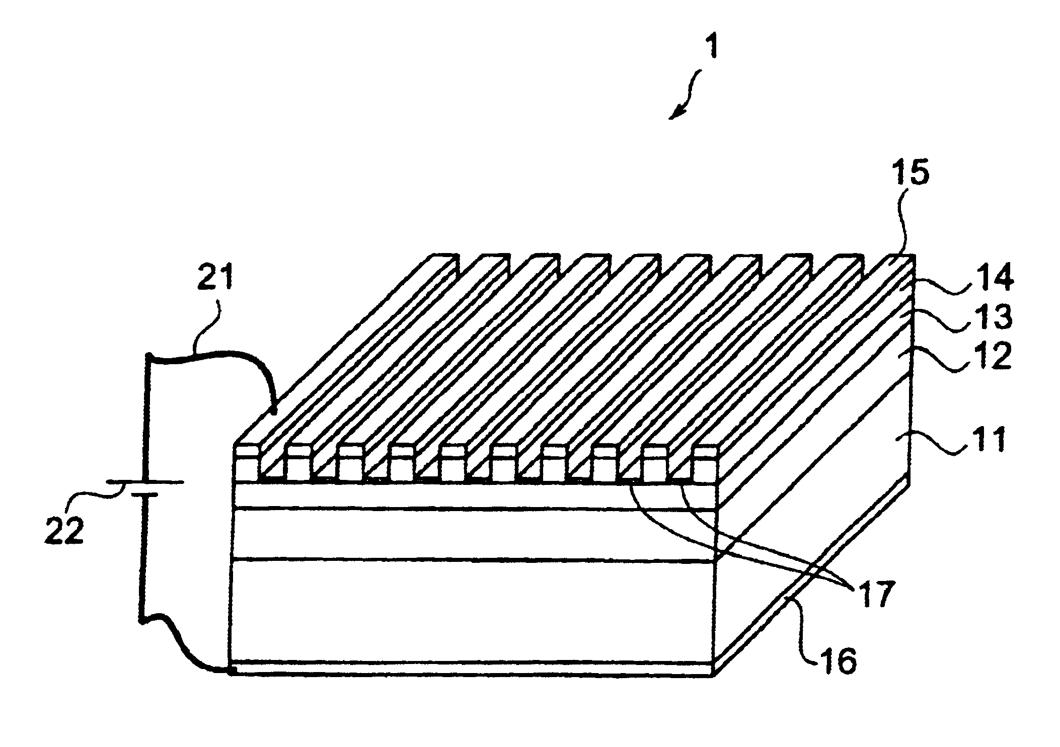
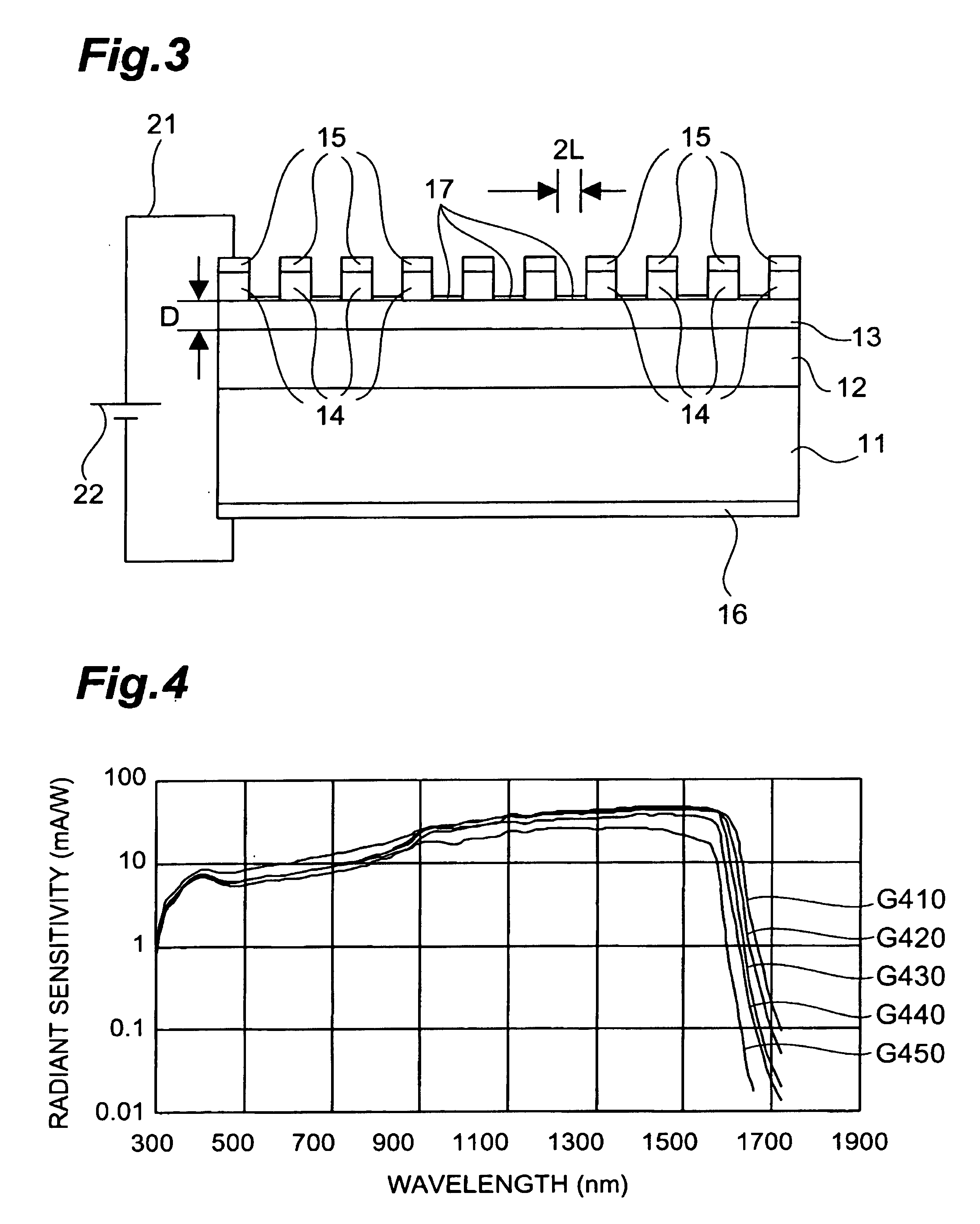
[0031]FIG. 2 is an entire perspective view of an embodiment of a photocathode according to the present invention, and FIG. 3 is a cross sectional view on the photocathode shown in FIG. 2.

[0032]As shown in FIG. 2, a photocathode 1 according to the present embodiment comprises a substrate 11 composed of p-type InP and having a carrier density of 1018 cm−3 or higher. A light absorbing layer 12 is formed on the upper layer of the substrate 11. The light absorbing layer 12 is composed of p-type InGaAs and has a carrier density of 1016 cm−3 and a thickness of 2 μm.

[0033]An electron emitting layer 13 for accelerating photoelectrons towards the emitting surface is formed on the upper layer of the light absorbing layer 12. The electron emitting layer 13 is composed of p-type InP and has a carrier density of 1016 cm−3 and a thickness of 0.7 μm. A contact layer 14 is formed on the upper layer of the el...


PUM


Abstract

The invention relates to a photocathode having a structure that permits a decrease in the radiant sensitivity at low temperatures is suppressed so that the S/N ratio is improved. In the photocathode, a light absorbing layer is formed on the upper layer of a substrate. An electron emitting layer is formed on the upper layer of the light absorbing layer. A contact layer having a striped-shape is formed on the upper layer of the electron emitting layer. A surface electrode composed of metal is formed on the surface of the contact layer. The interval between bars in the contact layer is adjusted so as to become 0.2 μm or more but 2 μm or less.

Description

BACKGROUND OF THE INVENTION[0001]1. Field of the Invention[0002]The present invention relates to a photocathode (photoelectron emitting surface) for emitting photoelectrons in response to photon incidence.[0003]2. Related Background Art[0004]A photocathode comprising a light absorbing layer and an electron emitting layer provided on a semiconductor, and means for applying an electric field between these light absorbing layer and electron emitting layer is disclosed, for example, in Japanese Patent No. 2923462 (Reference 1). This photocathode comprises a substrate composed of InP. A light absorbing layer composed of InGaAs having a thickness of 2 μm is formed on the upper layer of the substrate, while a p-type InP electron emitting layer having a thickness of 0.7 μm is formed on the light absorbing layer. Further, a mesh-shaped electrode comprising an n-type InP layer and a Ti metal layer for providing a potential to this n-type InP layer is formed on the p-type InP electron emitting...

Claims


Application Information

Patent Timeline
Patent Type & Authority Patents(United States)
IPC IPC(8): H01L29/06H01J40/06H01J40/00H01J1/02H01J1/34H01L29/02H01L33/00H01J43/08
CPCH01J1/34H01J2201/342
Inventor HIROHATA, TORUNIIGAKI, MINORUMOCHIZUKI, TOMOKOYAMADA, MASAMI
Owner HAMAMATSU PHOTONICS KK
Why Eureka
Try Eureka