Variable quality semiconductor film substrate
- Summary
- Abstract
- Description
- Claims
- Application Information
AI Technical Summary
Benefits of technology
Problems solved by technology
Method used
Image

Examples
Embodiment Construction
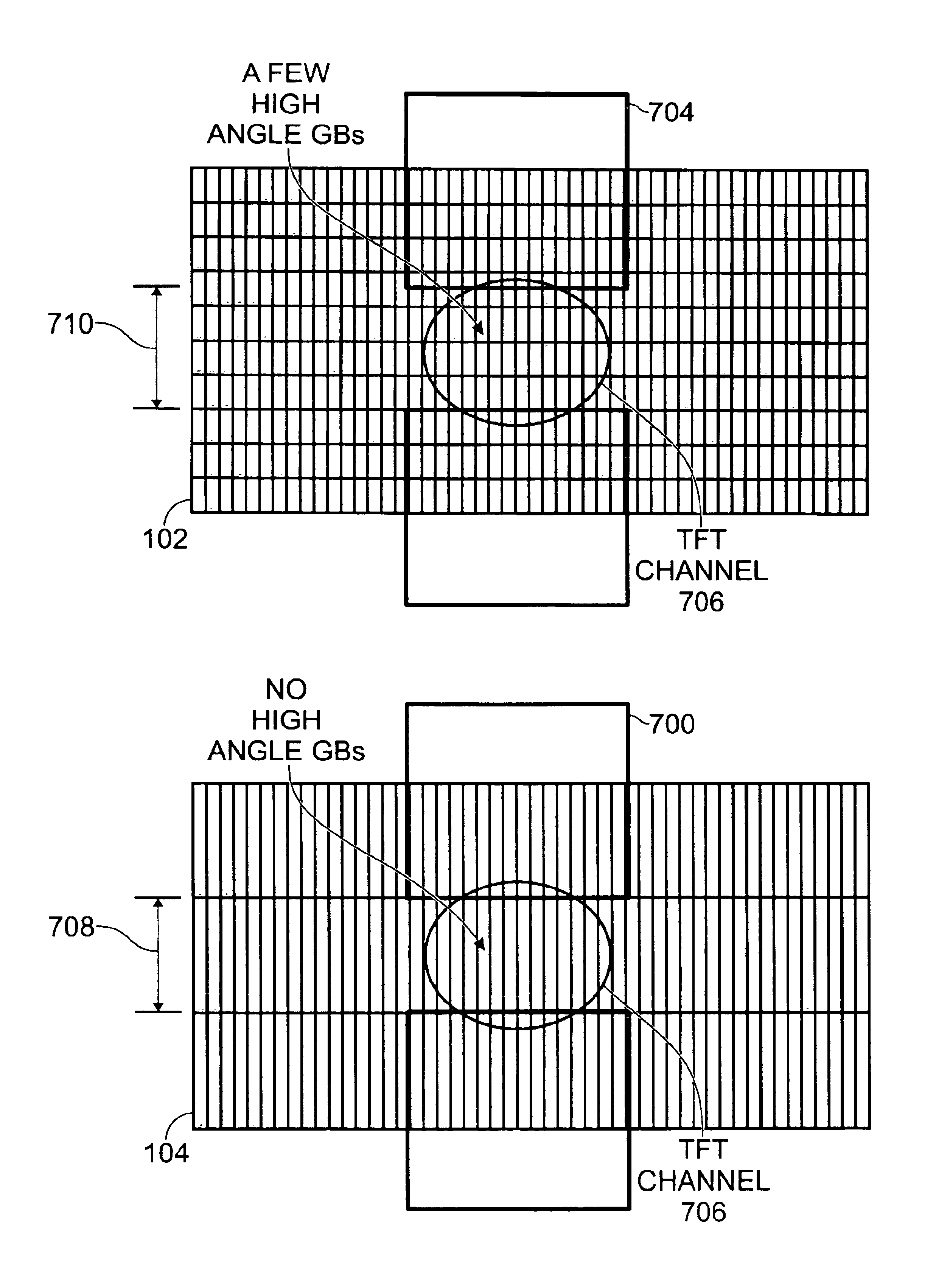
[0031]FIG. 4 is a plan view of the present invention variable quality semiconductor film substrate. The substrate 100 comprises a first area 102 with semiconductor film including crystalline material having a first lattice mismatch between adjacent crystal domains, and a second area 104 with semiconductor film including crystalline material having a second lattice mismatch between adjacent crystal domains, less than the first lattice mismatch. Of particular interest are silicon substrates used in the formation of TFTs of a substrate that makes up the panel of an LCD. Shown are a plurality of areas with semiconductor film including crystalline material, each area having a particular degree of lattice mismatch between adjacent crystal domains.
[0032]More specifically, a first area (region 1) 102, a second area (region 2) 104, a third area (region 3) 106, and a fourth area (region 4) 108 are shown. The first area 102 is associated with a first mask, or a first mask pattern. Likewise, th...
PUM
 Abstract
Description
Claims
Application Information
 - R&D Engineer
- R&D Manager
- IP Professional
- Industry Leading Data Capabilities
- Powerful AI technology
- Patent DNA Extraction
Browse by: Latest US Patents, China's latest patents, Technical Efficacy Thesaurus, Application Domain, Technology Topic.
© 2024 PatSnap. All rights reserved.Legal|Privacy policy|Modern Slavery Act Transparency Statement|Sitemap