

Silicon rich barrier layers for integrated circuit devices
a technology of integrated circuit devices and barrier layers, which is applied in the direction of semiconductor devices, electrical appliances, basic electric elements, etc., can solve the problems of unwanted threshold voltage (vsub>t/sub>) shift in the semiconductor, and achieve the effect of preventing cross diffusion and penetration
- Summary
- Abstract
- Description
- Claims
- Application Information
AI Technical Summary
Benefits of technology
Problems solved by technology
Method used
Image

Examples
Embodiment Construction
[0014]In the following detailed description of the preferred embodiments, reference is made to the accompanying drawings that form a part hereof, and in which is shown by way of illustration, and not by way of limitation, specific preferred embodiments in which the invention may be practiced. It is to be understood that other embodiments may be utilized and that logical, mechanical, and electrical changes may be made without departing from the spirit and scope of the present invention.
[0015]It shall be observed that the process steps and structures described herein do not form a complete process flow for manufacturing integrated circuits. The present invention can be practiced in conjunction with a variety of integrated circuit fabrication techniques, including those techniques currently used in the art. As such, commonly practiced process steps are included in the description herein only if those steps are necessary for an understanding of the present invention.
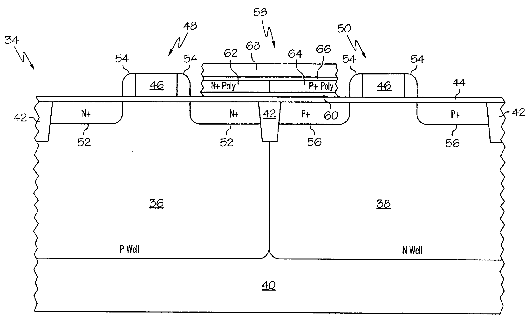
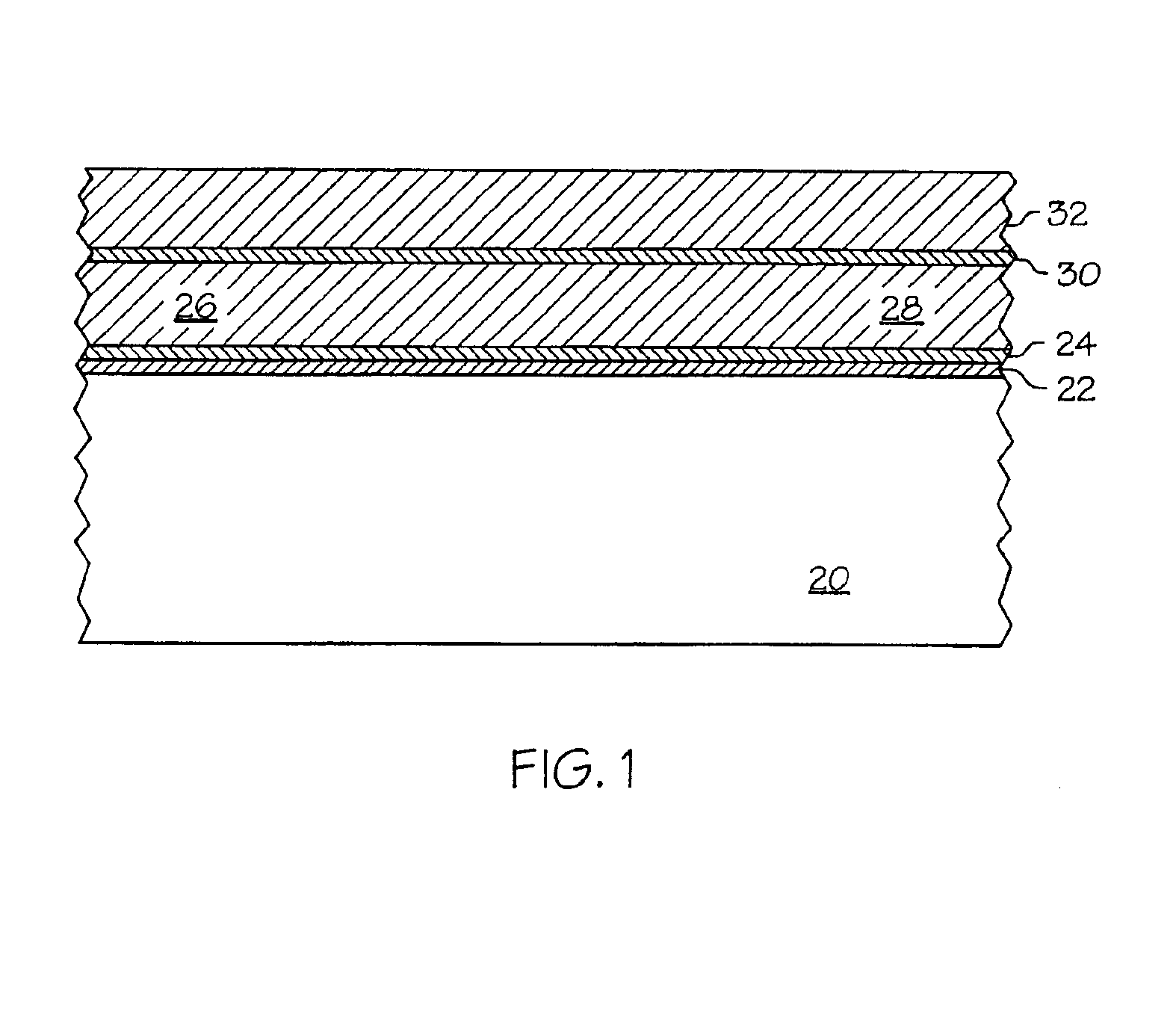
[0016]In FIG. 1, a p...
PUM
 Abstract
Description
Claims
Application Information