Method of writing to an organic memory

Inactive Publication Date: 2005-06-07
POLYIC
View PDF82 Cites 87 Cited by
  • Summary
  • Abstract
  • Description
  • Claims
  • Application Information

AI Technical Summary

Benefits of technology

[0015]A further possible means of writing to the memory having an organic basis consists in modifying the dielectric constant of the gate oxide. In this situation, the isolating layer between gate and semiconductor is

Problems solved by technology

The solutions offered by semiconductor technology are over-qualified and above all too costly for the requirements of these mass-produced articles.

Method used


Image

  • Method of writing to an organic memory
  • Method of writing to an organic memory
  • Method of writing to an organic memory

Examples


Embodiment Construction

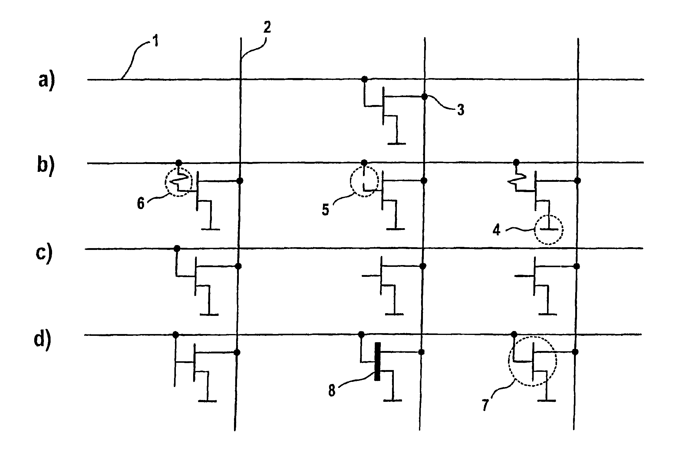
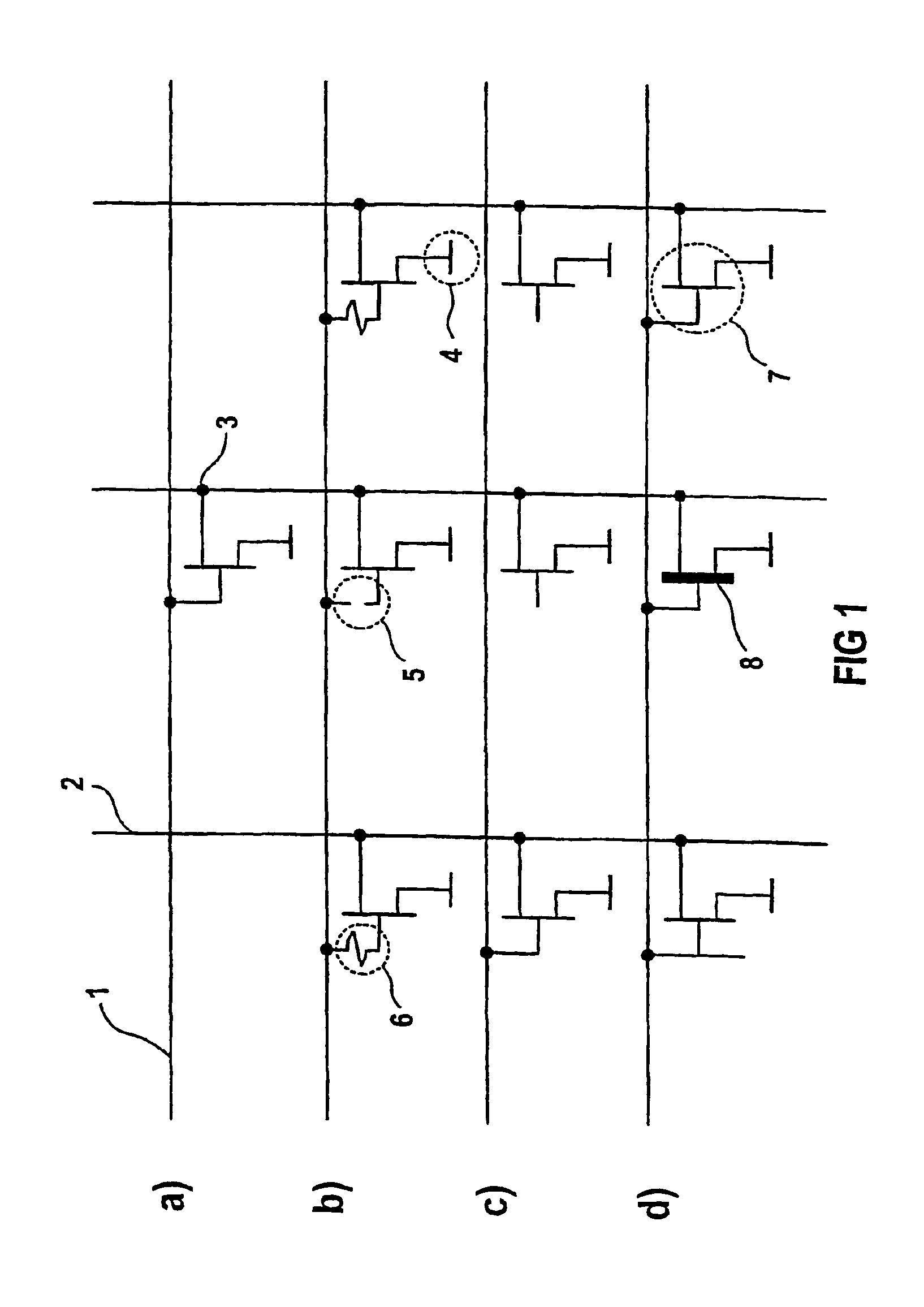
[0039]FIG. 1 shows a schematic circuit diagram of four embodiments of a memory matrix.

[0040]The circuit a) shows the programming through omission of the corresponding transistors of an integrated circuit for example;[0041]b) shows a so-called fusable link, whereby several conductor tracks are interrupted by a current surge and / or laser light or in some other manner (see there, middle field);[0042]c) shows the mask programming, whereby conductor tracks are either connected or not, in other words the transistor is connected or not connected, and[0043]d) shows the embodiment having different gate thicknesses which are conducting or non-conducting.

[0044]The horizontal lines 1 and the vertical lines 2 represent the electrical lines of the circuit. The points 3 serve to mark the fact that two crossing conductor tracks are in electrical contact with one another. The circuit symbol 7 represents a field effect transistor and shows the three terminals: source, drain and gate. The “T pieces”4 ...


PUM


Abstract

The invention relates to a memory, based on organic material and applied in combination with an organic integrated circuit (integrated plastic circuit). The invention particularly relates to a memory for a RFID-Tag (RFID-tags: radio frequency identification tags) and several methods for describing a memory.

Description

CROSS REFERENCE TO RELATED APPLICATIONS[0001]This is the 35 U.S.C. 371 National Stage of International Application PCT / DE01 / 03400 filed on Sep. 5, 2001, which designated the United States of America.FIELD OF THE INVENTION[0002]The invention relates to a memory, based on organic material and applied in combination with an organic integrated circuit (integrated plastic circuit). The invention particularly relates to a memory for an RFID tag (RFID tags: radio frequency identification tags) and a plurality of methods for writing to a memory.BACKGROUND OF THE INVENTION[0003]Organic integrated circuits based on organic field effect transistors (OFETs) are used for high-volume microelectronics applications and disposable products such as contactless readable identification and product tags, where the excellent operating characteristics of silicon technology can be sacrificed in favor of guaranteeing mechanical flexibility and very low manufacturing costs. The components such as electronic ...

Claims


Application Information

Patent Timeline
IPC IPC(8): G11C13/02G11C17/00G11C17/08G06K19/07G06K19/077G11C13/00G11C17/14H01L27/10H01L27/28H01L51/05
CPCB82Y10/00G11C17/00G11C13/0014
Inventor BERNDS, ADOLFCLEMENS, WOLFGANGFIX, WALTERLORENZ, MARKUSROST, HENNING
Owner POLYIC
Why Eureka
Try Eureka