Light emitting device and manufacturing method thereof

Inactive Publication Date: 2005-06-14
SEMICON ENERGY LAB CO LTD
View PDF37 Cites 55 Cited by
  • Summary
  • Abstract
  • Description
  • Claims
  • Application Information

AI Technical Summary

Benefits of technology

[0015]The object of the present-invention is to prevent a deterioration of a film deposition of an organic compound layer formed on an electrode by forming the structure that seldom has a difference of level between an electrode formed face and an electrode when an electrode is formed in manufacturing step of a light emitting device. Further, a structure in which concentration of electrical field is never occurred is manufactured thereby enabling to provide a long-living light emitting device in which the light emitting element is hardly deteriorated.
[0019]The first electrode and the leveled insulating layer can be formed on the same plane, and deterioration and film forming irregularities that follow electric field concentration of the organic compound layer formed on the first electrode can be prevented, in accordance with the above structure. Note that a state in which a conductive film that becomes the first electrode has been patterned is referred to as a conductor within this specification, and that the conductor is referred to as the first electrode after undergoing the polishing process by the CMP method. In addition, the insulating film formed so as to cover the conductor is referred to as the leveled insulating layer after undergoing polishing process by the CMP method.
[0021]Additionally, although it is necessary to form the second electrode by using a transparent conductive film having light transmitting characteristics when forming an upper surface emission structure, sputtering damage during film formation of the second electrode can be prevented by forming the second electrode using evaporation and by forming a barrier film in advance.
[0022]Furthermore, with the elements of the present invention, the second electrode can be formed without causing film forming irregularities, even if it is necessary to form a thin film due to qualities such as material transmittivity and resistivity when forming the second electrode in order to give it a flat structure.
[0082]Steps between the first electrode and the insulating film are thus eliminated, and therefore problems such as film formation irregularities arising upon forming an organic compound layer and a second electrode later can be resolved.
[0083]In addition, by performing the aforementioned processing using the CMP method, the film thickness of the organic compound layer formed on the first electrode can be made uniform because the surface of the first electrode is leveled, and an electric field can be added uniformly with respect to the organic compound layer. Note that electric current density is non-uniform in the organic compound layer in the case where the electric field is non-uniform, and not only does the luminance of a light emitting element drop, but in addition, a problem arises in that the element lifetime is reduced because the element deteriorates quickly. Processing by the CMP method therefore also has an effect of increasing the element characteristics by allowing the addition of a uniform electric field with respect to the organic compound layer.

Problems solved by technology

There is a danger that an electric field concentration may occur from an edge portion of a first electrode, and an organic compound layer formed on the first electrode may deteriorate, and there is a danger that film formation irregularities may develop when forming the organic compound layer due to roughness formed when there is a step in the edge portion of the first electrode, and when the edge portion of the first electrode is covered by an insulating film.

Method used


Image

  • Light emitting device and manufacturing method thereof
  • Light emitting device and manufacturing method thereof
  • Light emitting device and manufacturing method thereof

Examples


embodiment mode 1

[Embodiment Mode 1]

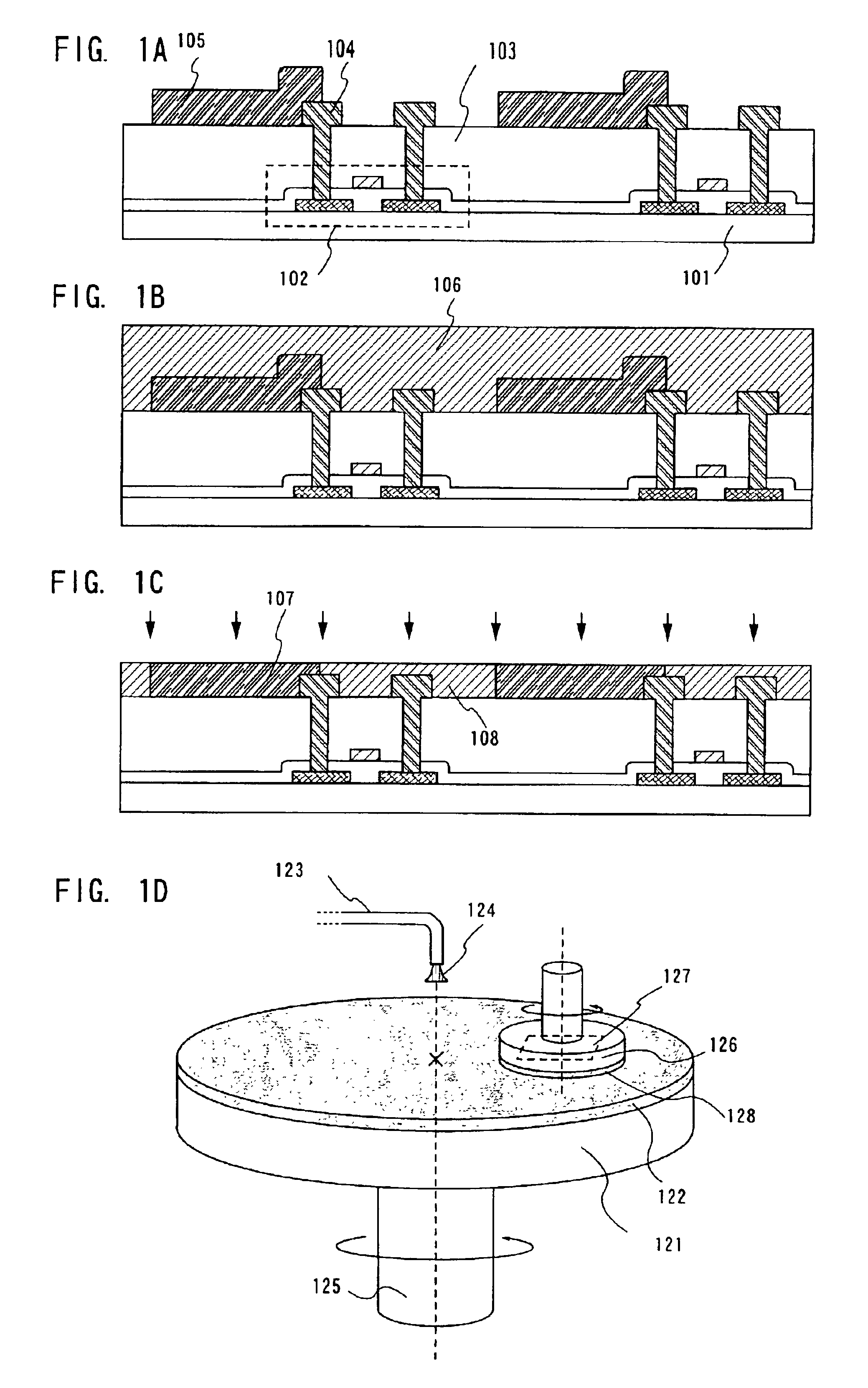
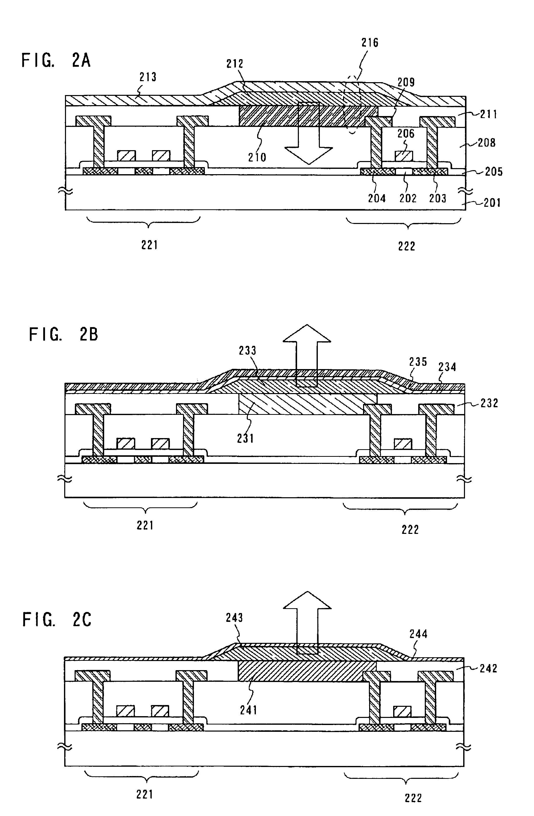
[0114]A cross sectional structure of a pixel portion of a light emitting device formed as Embodiment Mode 1 of the present invention is shown in FIG. 2A.

[0115]Thin film transistors (TFTs) are formed on a substrate 201 in FIG. 2A. Note that there are shown here, an electric current control TFT 222 which is electrically connected to a first electrode 210 of a light emitting element 216, and which has a function for controlling electric current supplied to the light emitting element 216, and a switching TFT 221 for controlling a video signal applied to a to gate electrode of the electric current control TFT 222.

[0116]A glass substrate is used for the substrate 201 as a substrate having light transmittance here, and a quartz substrate may also be used. Further, active layer of each TFT is provided with at least a channel forming region 202, a source region 203, and a drain region 204.

[0117]Further, a gate electrode 206 is formed covering a gate insulating film 205, an...

embodiment mode 2

[Embodiment Mode 2]

[0122]The following describe a sectional structure of a pixel portion of a light emitting device as Embodiment Mode 2 of the present invention, referring to FIG. 2B. The structure is formed is the same as in Embodiment Mode 1 except that the current-controlling TFT 222 is formed by an n-channel type. Thus, the structure formed after that the wiring 209 is formed is described.

[0123]On the first interlayer insulating film 208 is formed a first electrode 231 connected electrically to the source region or the drain region of the current-controlling TFT 222 by the wiring 209. In Embodiment Mode 2, the first electrode 231 is formed to be a cathode.

[0124]The organic compound layer 233 is formed on the first electrode 231, therefore, it is allowable to form a barrier layer 234 by a sputtering for preventing the damage of the organic compound layer 233 when the second electrode 235 is formed. For the barrier layer 234, copper phthalocyanine (Cu-Pc), gold, platinum or the l...

embodiment mode 3

[Embodiment Mode 3]

[0128]The following describe a sectional structure of a pixel portion of a light emitting device as Embodiment Mode 3 of the present invention with reference to FIG. 2C. The current-controlling TFT 222 is formed to be a p-channel type as same as in the Embodiment Mode 1. Thus, the structure formed after that the wiring 209 is formed is described.

[0129]On the first interlayer insulating film 208 is formed a first electrode 241 connected electrically to the source region or the drain region of the current-controlling TFT 222 by the wiring 209. In Embodiment Mode 3, the first electrode 241 is formed to be an anode. For forming the first electrode 241, a material having a large work function and functioning as an anode is used. Further, conductive materials having light-shielding effect and a high reflectivity are used to form the first electrode 241.

[0130]An organic compound layer 243 is deposited on the first electrode 241. A light emitting elements made of the seco...


PUM

PropertyMeasurementUnit
Thicknessaaaaaaaaaa
Electrical conductivityaaaaaaaaaa
Structureaaaaaaaaaa

Abstract

An element structure is provided in which film formation irregularities and deterioration of an organic compound layer formed on an electrode are prevented in an active matrix light emitting device. After forming an insulating film so as to cover edge portions of a conductor which becomes a light emitting element electrode, polishing is performed using a CMP (chemical mechanical polishing) method in the present invention, thus forming a structure in which surfaces of a first electrode and a leveled insulating layer are coplanar. The film formation irregularities in the organic compound layer formed on the electrode can thus be prevented, and electric field concentration from the edge portions of the electrode can be prevented.

Description

BACKGROUND OF THE INVENTION[0001]1. Field of the Invention[0002]The present invention relates to a light emitting device with a light emitting element that emits fluorescent light or phosphorescent light upon application of electric field to a pair of electrodes of the element which sandwich a film containing an organic compound (the film is hereinafter referred to as organic to compound layer), and to a method of manufacturing the light emitting device. Incidentally, in the present specification, the light emitting device indicates an image display device or a plane emission device using a light emitting element as a light emitting element. Besides, the light emitting device includes a module in which a FPC (Flexible Printed Circuit), a TAB (Tape Automated Bonding) tape, or a TCP (Tape Carrier Package) is attached to a substrate over which a light emitting element is formed, a module in which a printed wiring board is provided at an end of a TAB tape or a TCP, and a module in which...

Claims


Application Information

Patent Timeline
IPC IPC(8): H01L21/336H01L29/786H01L21/02H01L27/32H01L29/66H01L27/28H01L51/52H01L21/321H01L21/3105H01L51/50H01L51/05H01L51/30H05B33/10G09F9/00G09F9/30H01L51/00H05B33/22H05B33/28
CPCH01L27/3244H01L29/66757H01L29/78636H01L51/5206H01L51/5221H01L51/5234H01L21/31051H01L2251/558H01L27/3246H01L29/78645H01L51/005H01L51/0059H01L51/0078H01L51/0084H01L51/5016H01L51/5203H01L2251/5315H01L21/3212H10K59/122H10K59/12H10K85/60H10K85/631H10K85/311H10K85/341H10K50/11H10K2101/10H10K50/81H10K50/828H10K2102/3026H10K2102/351H10K59/805H10K50/805
Inventor KONUMA, TOSHIMITSU
Owner SEMICON ENERGY LAB CO LTD
Why Eureka
Try Eureka