Method of manufacturing a multi-layer semiconductor nanoparticle, and a multi-layer semiconductor nanoparticle manufactured by the method

Inactive Publication Date: 2005-06-28
HITACHI SOFTWARE ENG
View PDF6 Cites 39 Cited by
  • Summary
  • Abstract
  • Description
  • Claims
  • Application Information

AI Technical Summary

Benefits of technology

[0021]When excited, the multi-layer semiconductor nanoparticle manufactured according to the method of the invention may emit fluorescence having a peak in a narrow wavelength-

Problems solved by technology

However, the semiconductor nanoparticles obtained by the above method exhibit a wide grain-size distribution and therefore cannot provide the full advantage of the properties of semiconductor nanoparticles.
Semiconductor nanoparticles obtained by these methods exhibit a spectrum with a relatively narrow wavelength-width peak, however, even in such a monodisperse state, the light-emission characteristics of the crystal are not quite satisfactory.
However, it has been difficult to combine the former and the latter techniques into one process because of the difference in the stabilizer used.

Method used


Image

  • Method of manufacturing a multi-layer semiconductor nanoparticle, and a multi-layer semiconductor nanoparticle manufactured by the method
  • Method of manufacturing a multi-layer semiconductor nanoparticle, and a multi-layer semiconductor nanoparticle manufactured by the method
  • Method of manufacturing a multi-layer semiconductor nanoparticle, and a multi-layer semiconductor nanoparticle manufactured by the method

Examples


examples

[0027]The invention will be hereafter described by way of examples.

Preparation of a Semiconductor Nanoparticle

[0028]The present example employs one of a variety of methods for preparing semiconductor nanoparticles.

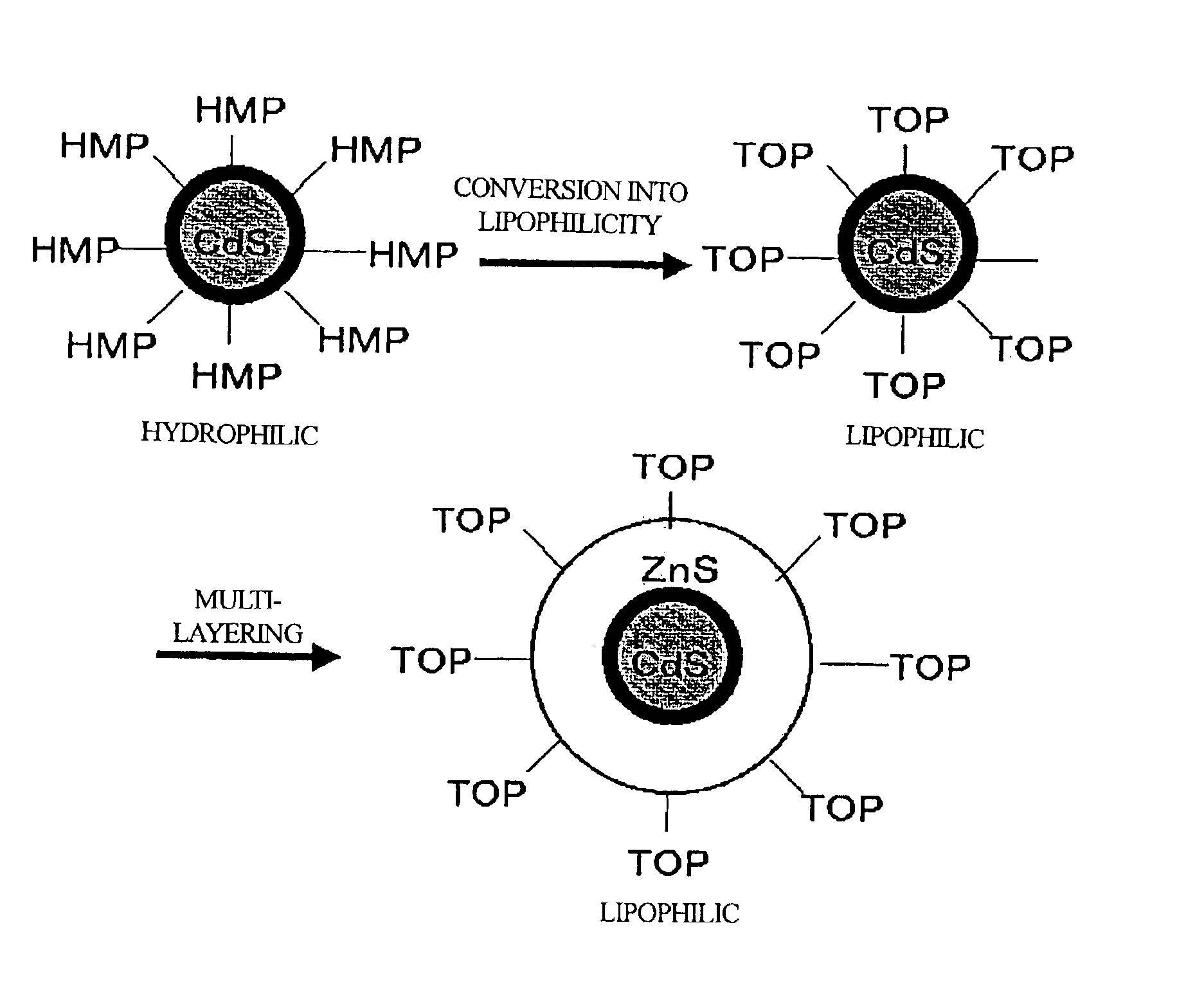
[0029]In a semiconductor nanoparticle, the proportion of its surface area to its volume is very large. As a result, semiconductor nanoparticles tend to coalesce very easily. In order to allow the semiconductor nanoparticles to exist stably, measures have to be taken to prevent them from colliding or fusing with each other. A variety of measures have been devised so far, which can be roughly divided into two types. One is the physical isolation of the semiconductor nanoparticles by placing them in a solid matrix and a polymer matrix. The other is the inactivation of the particle surface by chemically modifying the metal-ion site on the particle surface with a low-molecule organic matter having a high level of ability to form a complex with the metal-ion site.

[0030]Based on ...


PUM


Abstract

Multi-layered semiconductor nanoparticles having a very narrow grain-size distribution and exhibiting a spectrum having a narrow wavelength-width peak are prepared by a manufacturing method combining a monodisperse semiconductor nanoparticle manufacturing method and a multi-layer semiconductor nanoparticle preparation method. The nature of a solution of monodisperse semiconductor nanoparticles that is stabilized by a surface stabilizer is transformed between hydrophilic and lipophilic by substituting the surface stabilizer. The stabilized semiconductor nanoparticles are then shifted between an aqueous layer and an organic layer. The semiconductor nanoparticles are coated with multiple layers in the organic layer, and the organic layer is drawn off to recover the semiconductor nanoparticles therefrom.

Description

BACKGROUND OF THE INVENTION[0001]1. Technical Field[0002]The present invention relates to a method of manufacturing a multi-layer semiconductor nanoparticle that emits fluorescence of a narrow wavelength width, and the multi-layer semiconductor nanoparticle manufactured by the method.[0003]2. Background Art[0004]Semiconductor nanoparticles of a grain size of 10 nm or less are located in the transition region between bulk semiconductor crystals and molecules. Their physicochemical properties are therefore different from both bulk semiconductor crystals and molecules. In this region, the energy gap of a semiconductor nanoparticle increases as its grain size decreases, due to the appearance of a quantum-size effect. In addition, the degeneracy of the energy band that is observed in bulk semiconductors is removed and the orbits are dispersed. As a result, a lower-end of the conduction band is shifted to the negative side and an upper-end of the valence band is shifted to the positive si...

Claims


Application Information

Patent Timeline
IPC IPC(8): C09C3/08C09C3/00C09C3/06H01L33/00C01G11/02B82Y20/00B82Y30/00C09K11/56
CPCB82Y5/00B82Y30/00C09C3/006C09C3/08C30B7/00C30B7/005C09C3/06C01P2004/52C01P2004/84C01P2006/60Y10S977/715H01L33/20Y10S977/89
Inventor SATO, KEIICHIKUWABATA, SUSUMU
Owner HITACHI SOFTWARE ENG
Why Eureka
Try Eureka