
Method of depositing a TaN seed layer

Inactive Publication Date: 2005-06-28
APPLIED MATERIALS INC
View PDF35 Cites 60 Cited by
  • Summary
  • Abstract
  • Description
  • Claims
  • Application Information

AI Technical Summary

Benefits of technology

[0020]In another embodiment of the method of forming a TaN seed layer, a tantalum film is deposited on a semiconductor substrate surface, and then the surface of the Ta film is bombarded with high energy species while in contact with a nitrogen-containing plasma. Small amounts of reactive tantalum species, which are liberated from the tantalum film surface due to the high energy species bombardment, react with or trap nitrogen from a plasma present over the tantalum film surface, and redeposit on the tantalum film surface to provide a TaN seed layer, having a nominal nitrogen content between about 5 atomic % and about 33 atomic %, and typically less than about 15 atomic %. After formation of at least two monolayers of TaN seed layer material, nitrogen is removed from the plasma present over the TaN seed layer surface. Tantalum subsequently deposited over the TaN seed layer surface is alpha-tantalum. The TaN seed layer typically ranges from about 2 monolayers to about 10 monolayers, which provides a TaN seed layer thickness ranging from about 20 Å to about 100 Å. The plasma density and the voltage on the substrate surface are controlled so that the amount of energy transferred to the Ta film surface is sufficient to cause Ta species to rise into the space above the Ta film surface, where the nitrogen species from the plasma contact and react with the tantalum species. This forms TaN atoms, and the TaN atoms thus formed settle down on the Ta surface, forming a TaN seed layer. Controlling the plasma density and the voltage on the substrate enables applicants to control the amount of energy that is transferred to the substrate and ensures that the transferred energy is sufficient to provide Ta species for reaction with nitrogen in the plasma, without sputtering Ta from the Ta film surface onto adjacent non-tantalum containing surfaces. In general, resputtering does not occur or is minimal; typically, less than 10% of the original Ta film thickness is altered.

Problems solved by technology

Since the seed layer is typically about 2-10 monolayers thick, it is difficult to obtain precisely the desired nitrogen content in the seed layer.

Method used


Image

  • Method of depositing a TaN seed layer
  • Method of depositing a TaN seed layer
  • Method of depositing a TaN seed layer

Examples


Embodiment Construction

[0044]This application is a continuation in part of U.S. patent application Ser. No. 10 / 146,416, filed May 14, 2002 which is presently pending, and which is incorporated by reference herein in its entirety.

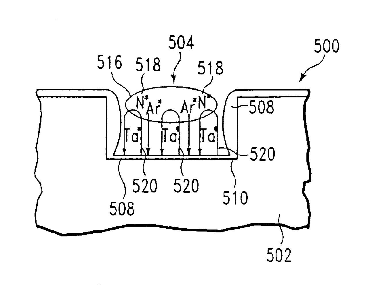
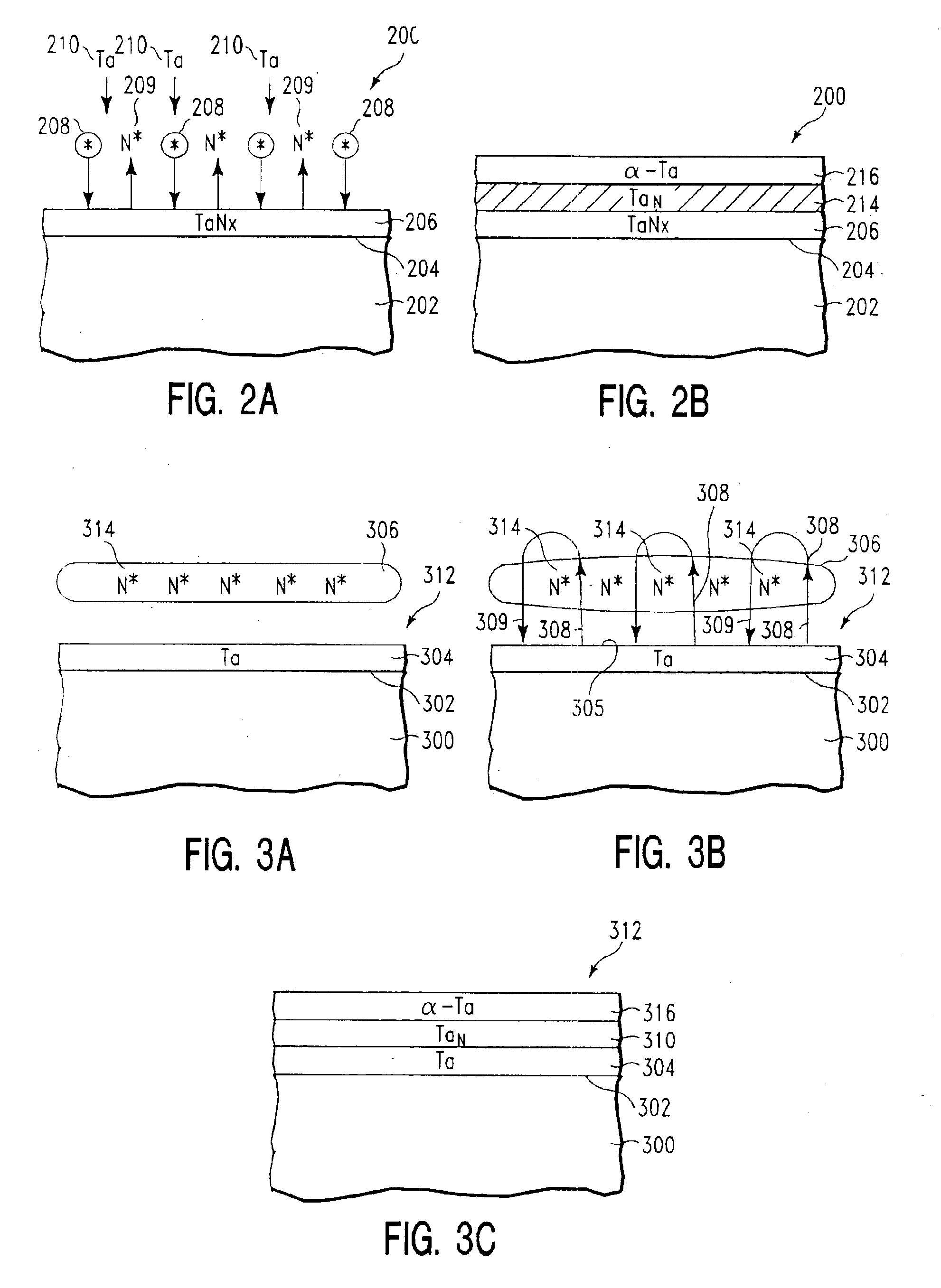
[0045]We originally discovered a surprising and easy method for depositing ultra-low resistivity (about 10 μΩ-cm) tantalum films.

[0046]Deposition of a 1,000 Å thick tantalum film using high density plasma or long-throw sputtering upon a silicon dioxide substrate, at a substrate support platen temperature of about 400° C. or higher (a substrate temperature of about 325° C. or higher), results in a tantalum film having a resistivity of about 10 μΩ-cm. (Deposition of thinner films under the same conditions provides the same low resistivity.) This is compared with a film resistivity of about 165 μΩ-cm obtained for a tantalum film sputtered upon a room temperature substrate. In addition, deposition of the tantalum film at room temperature, followed by a 15 minute anneal at a substrate ...


PUM

PropertyMeasurementUnit
Temperatureaaaaaaaaaa
Pressureaaaaaaaaaa
Pressureaaaaaaaaaa

Abstract

We have discovered a method of providing a thin approximately from about 20 Å to about 100 Å thick TaN seed layer, which can be used to induce the formation of alpha tantalum when tantalum is deposited over the TaN seed layer. Further, the TaN seed layer exhibits low resistivity, in the range of 30 μΩ m and can be used as a low resistivity barrier layer in the absence of an alpha tantalum layer. In one embodiment of the method, a TaN film is altered on its surface form the TaN seed layer. In another embodiment of the method, a Ta film is altered on its surface to form the TaN seed layer.

Description

[0001]This application is a continuation in part of the U.S. patent application Ser. No. 10 / 146,416, filed May 14, 2002, now abandoned; which is a continuation of U.S. patent application Ser. No. 09 / 770,934, filed Jan. 25, 2001, which is now U.S. Pat. No. 6,458,255; which is a continuation of U.S. patent application Ser. No. 09 / 160,638, filed Sep. 24, 1998, which is abandoned.BACKGROUND OF THE INVENTION[0002]1. Field of the Invention[0003]The present invention pertains to a method of depositing seed layers which induce the formation of alpha tantalum in a tantalum film which is deposited over the seed layer.[0004]2. Brief Description of the Background Art[0005]As microelectronics continue to miniaturize, interconnection performance, reliability, and power consumption has become increasingly important, and interest has grown in replacing aluminum alloys with lower resistivity and higher reliability metals. Copper offers a significant improvement over aluminum as a contact and interco...

Claims


Application Information

Patent Timeline
IPC IPC(8): C23C14/54C23C14/16C23C14/06H01L21/285H01L21/02H01L21/70H01L21/318H01L21/768C23C14/58
CPCC23C14/0641C23C14/165C23C14/541C23C14/5806H01L21/76876H01L21/318H01L21/76846H01L21/76856H01L21/76862H01L21/2855H01L21/0217
Inventor TANG, XIANMINGOPALRAJA, PRABURAMRENGARAJAN, SURAJFORSTER, JOHN C.FU, JIANMINGDING, PEIJUN
Owner APPLIED MATERIALS INC
Features
  • Generate Ideas
  • Intellectual Property
  • Life Sciences
  • Materials
  • Tech Scout
  • Unparalleled Data Quality
  • Higher Quality Content
  • 60% Fewer Hallucinations
Learn More