Interface layer for the fabrication of electronic devices

a technology of electronic devices and interface layers, applied in the field of interface layers for the fabrication of electronic devices, can solve the problems of poor adhesion of the layer, delaminate from the substrate, irregular formation of hillocks and/or pin holes, etc., and achieve the effect of promoting adhesion of the active device layer

Inactive Publication Date: 2005-06-28
KOVIO
View PDF31 Cites 74 Cited by
  • Summary
  • Abstract
  • Description
  • Claims
  • Application Information

AI Technical Summary

Benefits of technology

[0008]On top of the interface layer, an active device layer is formed. The active device layer is preferably a conducting layer. The interface layer preferably provides ohmic contact between the active device layer and the substrate such as a silicon-wafer or α-Si on glass and helps to promote adhesion of the active device layer to th...

Problems solved by technology

One of the shortcomings of fabricating thin conductive layers with liquids comprising metal-based materials, such as described above, is that the layers tend to exhibit poor adhesion and delaminat...

Method used


Image

  • Interface layer for the fabrication of electronic devices
  • Interface layer for the fabrication of electronic devices
  • Interface layer for the fabrication of electronic devices

Examples


Embodiment Construction

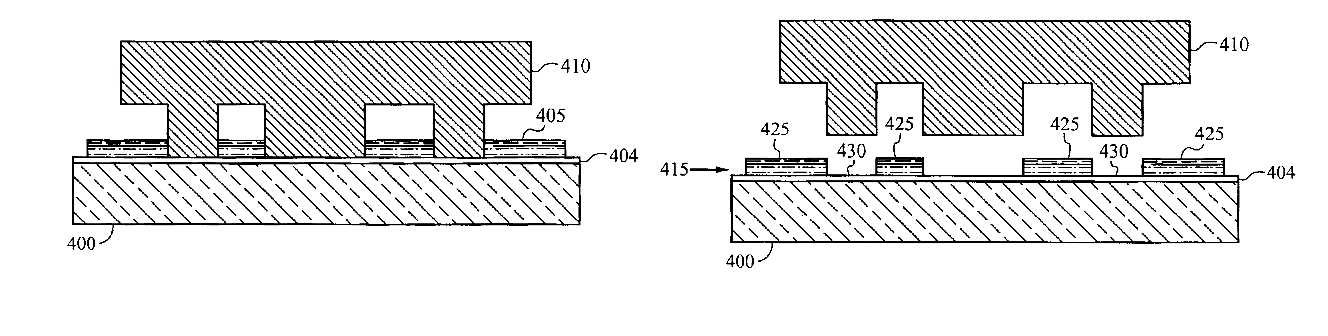
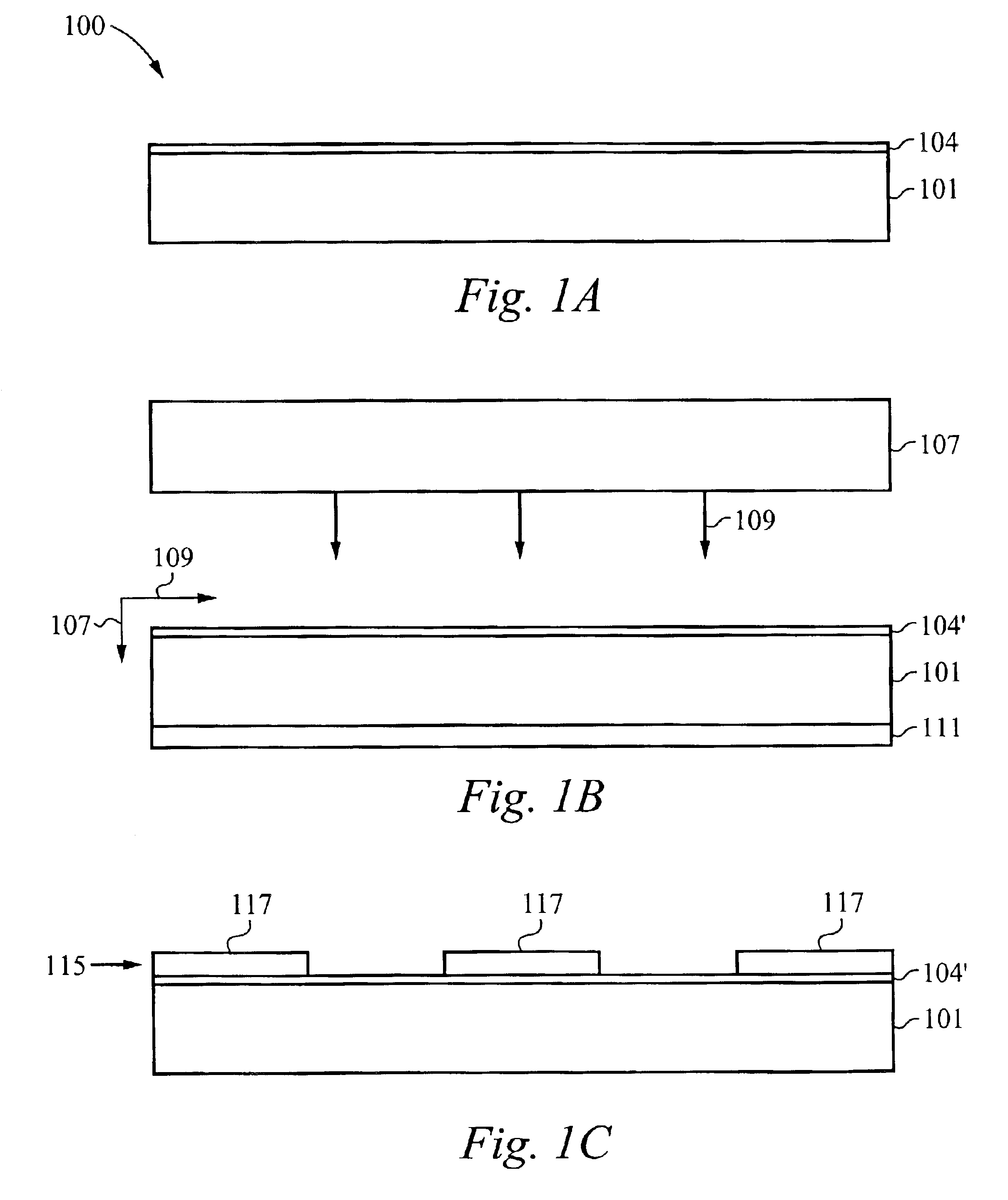
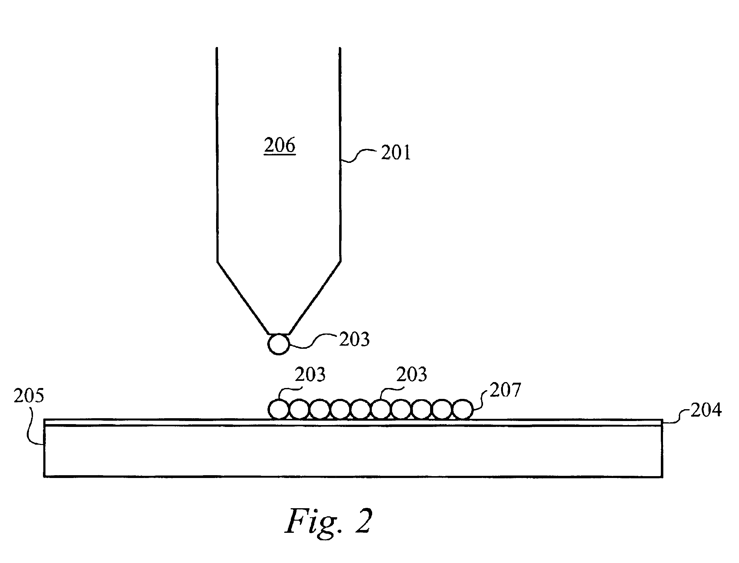
[0020]Referring to FIGS. 1a-b, in accordance with the embodiments of the invention, an interface layer 104′ (FIG. 1b) is formed by depositing a thin layer 104 of material comprising a suitable interface precursor onto a substrate 101. The substrate 101 is a silicon, quartz, glass, polymer, metal, or any other substrate suitable for the application at hand. The thin layer 104 can be deposited onto the substrate 101 using any number of methods including, slide bar coating, ink-jet coating, screen printing, dip coating and vapor deposition methods to name a few. Preferably, the thin layer 104 is deposited on the substrate 101 using spin coating techniques.

[0021]In accordance with the embodiments of the invention, the interface precursor comprises of one or more metals of Pd, Pt, Bi, Pb, Sn, Cu, Ni, W, Al, Cr, Ti, Co, Fe or Mo. The interface precursor is preferably an organometallic complex including, but not limited to metal carboxylates, alkoxides, alkyls, aryls, alkynes, alkenes, β-d...


PUM


Abstract

The present invention is directed to methods for making electronic devices with a thin anisotropic conducting layer interface layer formed between a substrate and an active device layer that is preferably patterned conductive layer. The interface layer preferably provides Ohmic and/or rectifying contact between the active device layer and the substrate and preferably provides good adhesion of the active device layer to the substrate. The active device layer is preferably fashioned from a nanoparticle ink solution that is patterned using embossing methods or other suitable printing and/or imaging methods. The active device layer is preferably patterned into an array of gate structures suitable for the fabrication of thin film transistors and the like.

Description

FIELD OF THE INVENTION[0001]The present invention relates to electronic devices. More specifically, the present invention relates to the method of fabricating electronic devices.BACKGROUND OF THE INVENTION[0002]Ultra-fine particles or nanoparticle (particles having an average diameter of 200 nanometers or less) are believed to be useful in the fabrication of microelectronic devices. Alivisatos et al., in U.S. Pat. No. 5,262,357, describe a method for making semiconductor nanoparticles from semiconductor precursors. Alivisatos et al. describe using these semiconductor nanoparticles to make continuous semiconductor films. Because the semiconductor nanoparticles exhibit significantly lower melting temperature than bulk materials, a layer of the semiconductor nanoparticles can be deposited on a substrate and annealed at relatively low temperatures, whereby the nanoparticles melt to form a continuous film.[0003]One of the goals for nanotechnology is to develop techniques and materials th...

Claims


Application Information

Patent Timeline
IPC IPC(8): H01L21/76H01L21/02H01L21/44H01L21/70H01L21/77
CPCH01L27/1292
Inventor HAUBRICH, SCOTTKUNZE, KLAUSDUNPHY, JAMES CGUDEMAN, CHRISROCKENBERGER, JOERGZURCHER, FABIOSLEIMAN, NASSRINTAKASHIMA, MAOSPINDT, CHRIS
Owner KOVIO
Why Eureka
Try Eureka