

Method of manufacturing a semiconductor device
a manufacturing method and semiconductor technology, applied in the direction of transistors, optics, instruments, etc., can solve the problems of lower manufacturing yield and higher manufacturing cost, and achieve the effect of small off-current and not requiring high alignment precision
- Summary
- Abstract
- Description
- Claims
- Application Information
AI Technical Summary
Benefits of technology
Problems solved by technology
Method used
Image

Examples
first embodiment
[0031]With reference to FIG. 1 and FIGS. 4A to 4I, a TFT and a liquid crystal display substrate using TFTs according to the invention will be described.
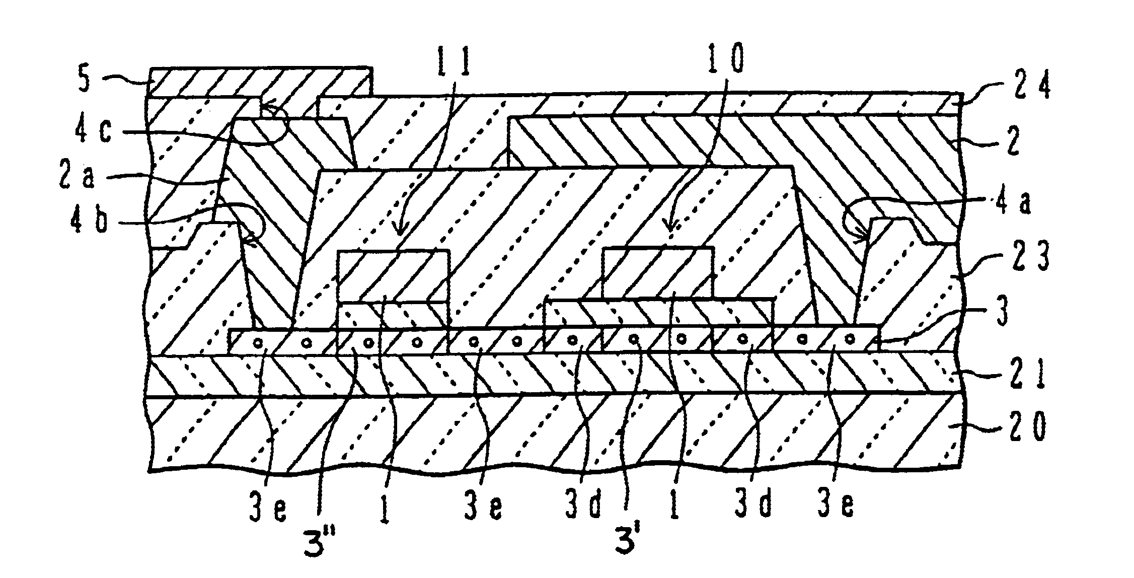
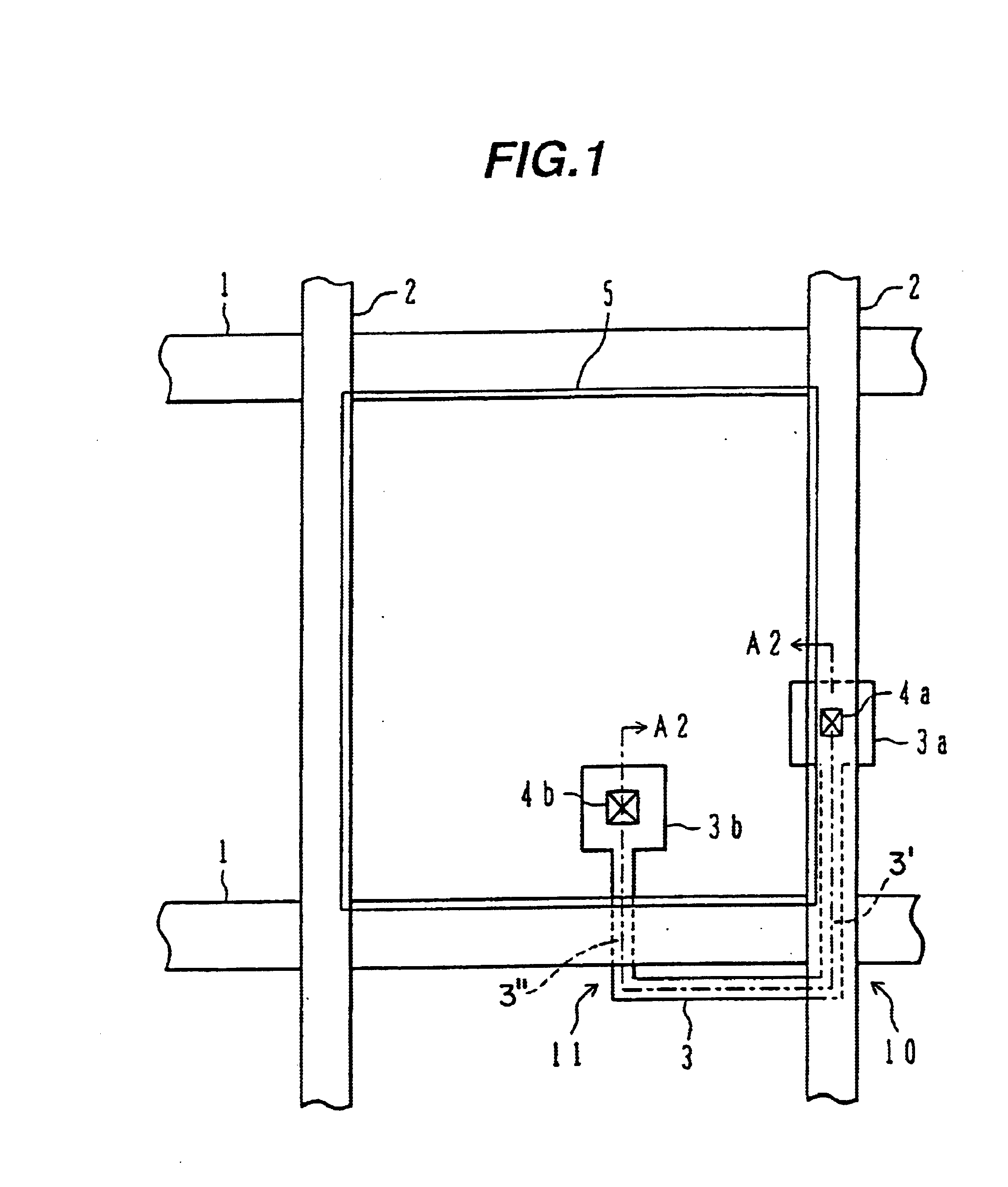
[0032]FIG. 1 is a plan view showing one pixel area of a liquid crystal display substrate according to the first embodiment. On an insulating principal surface of a glass substrate, a plurality of gate bus lines 1 and drain bus lines 2 are formed. Each gate bus line 1 extends in a row direction in FIG. 1, and each drain bus line extends in a column direction in FIG. 1. The gate bus line 1 and drain bus line 2 are electrically insulated in their cross areas.
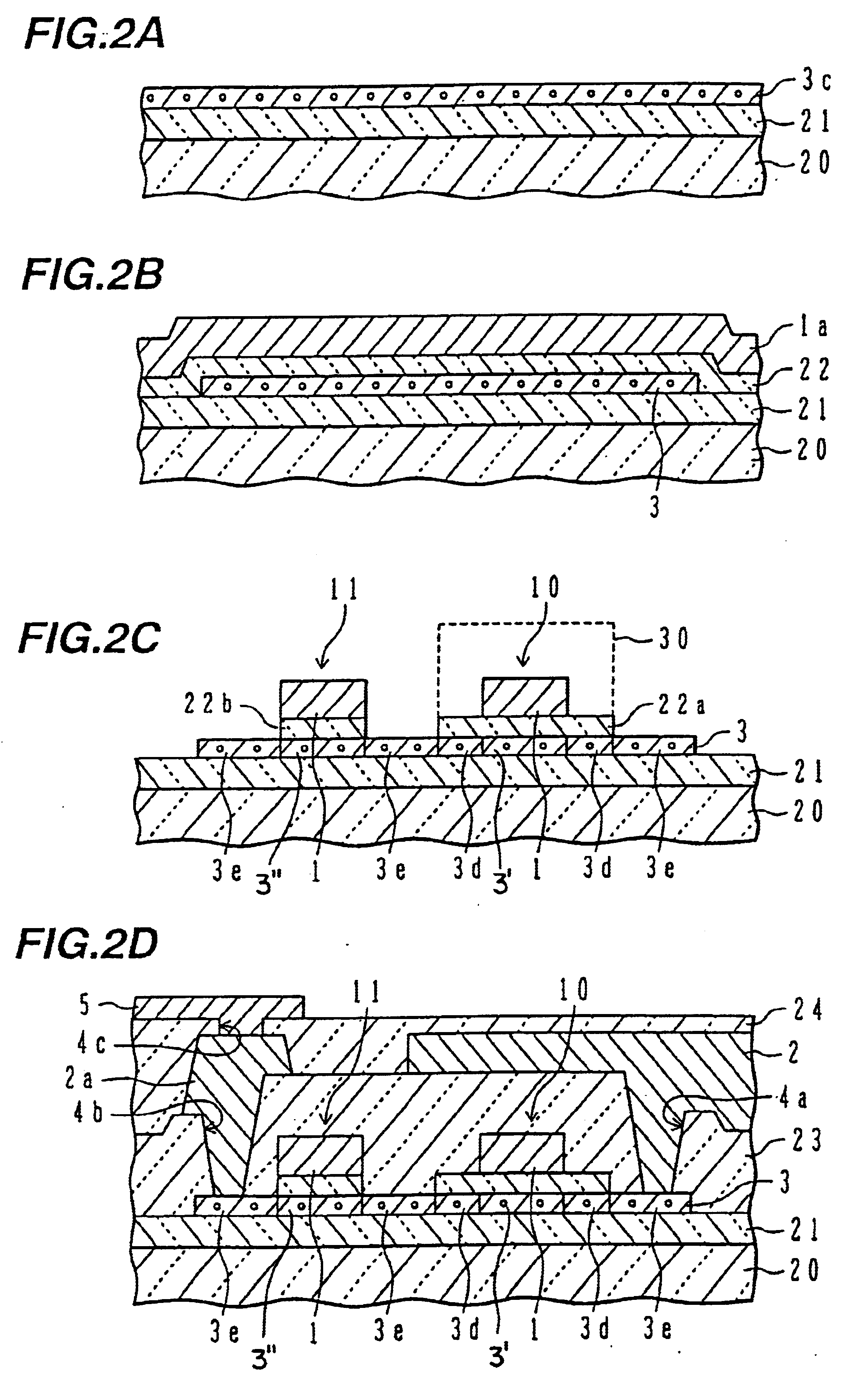
[0033]In each cross area between the gate bus line 1 and drain bus line 2, a current path pattern 3 made of polysilicon is disposed. One end portion 3a of the current path 3 is electrically connected to a corresponding drain bus line 2 via a contact hole 4a. The current path pattern 3 extends along the drain bus line 2 from the end portion 3a to a cross area 10 between the drain bus...
second embodiment
[0062]Next, with reference to FIGS. 6 and 7, a liquid crystal display substrate will be described.
[0063]FIG. 6 is a cross sectional view of a TFT used with the liquid crystal display substrate of the second embodiment. The principal surface of a glass substrate 20 has an underlie SiO2 film 21 formed thereon. A partial surface area of the underlie SiO2 film has a current path pattern 3 of polysilicon formed therein. The gate bus line 1 three-dimensionally crosses the current path pattern 3. A gate insulating film 22 is disposed between the gate bus line 1 and current path pattern 3. This structure is formed by the same processes as the processes up to the process of forming the gate bus line shown in FIG. 2C of the first embodiment.
[0064]Next, by using the gate bus line 1 as a mask, phosphorous ions are doped. The phosphorous ion doping conditions are the same as the conditions of the second phosphorous ion doping described with FIG. 2C of the first embodiment.
[0065]After phosphorou...
third embodiment
[0096]The cross sectional view of a substrate during the manufacture processes shown in FIG. 10A corresponds to FIG. 9A referred to for the description of the The current pattern 3 shown in FIG. 9A is replaced by an active region 60 of a single crystal silicon substrate shown in FIG. 10A, the gate insulating film 22 is replaced by a silicon oxide film 61 formed on the active region 60, the conductive film 1a is replaced by a conductive film 62, and the resist pattern 51 is replaced by a resist pattern 63.
[0097]As the processes similar to those shown in FIGS. 9B to 9E of the third embodiment are executed, a MISFET shown in FIG. 10B is obtained. This MISFET is constituted of source and drain regions 65, a gate insulating film 61a made of silicon oxide, and a gate electrode 62 made of AlSc alloy. Each of the source and drain regions 65 has the LDD structure including a low concentration region 65a and a high concentration region 65b.
PUM
| Property | Measurement | Unit |
|---|---|---|
| off-current | aaaaa | aaaaa |
| off-current | aaaaa | aaaaa |
| thickness | aaaaa | aaaaa |
Abstract
Description
Claims
Application Information