semiconductor memory

A memory and semiconductor technology, applied in the direction of semiconductor devices, static memory, read-only memory, etc., can solve the problems of increased chip area, small storage device circuit, etc., and achieve the effect of reducing leakage current, small turn-off current and increasing turn-on current

Active Publication Date: 2017-09-29
SHANGHAI HUAHONG GRACE SEMICON MFG CORP
View PDF5 Cites 0 Cited by
  • Summary
  • Abstract
  • Description
  • Claims
  • Application Information

AI Technical Summary

Problems solved by technology

However, since the split-gate flash memory has one more word line than the stacked-gate flash memory, the area of ​​the chip will also increase. In order to introduce memory cells with higher packing density into semiconductor memory devices, the design layout of the memory device circuits must also be changed accordingly. in smaller and smaller sizes

Method used


Image

  • semiconductor memory
  • semiconductor memory
  • semiconductor memory

Examples


Embodiment Construction

[0042] In order to make the content of the present invention clearer and easier to understand, the content of the present invention will be further described below in conjunction with the accompanying drawings. Of course, the present invention is not limited to this specific embodiment, and general replacements known to those skilled in the art are also covered within the protection scope of the present invention.

[0043] Secondly, the present invention is described in detail using schematic diagrams. When describing the examples of the present invention in detail, for the sake of illustration, the schematic diagrams are not partially enlarged according to the general scale, which should not be used as a limitation of the present invention.

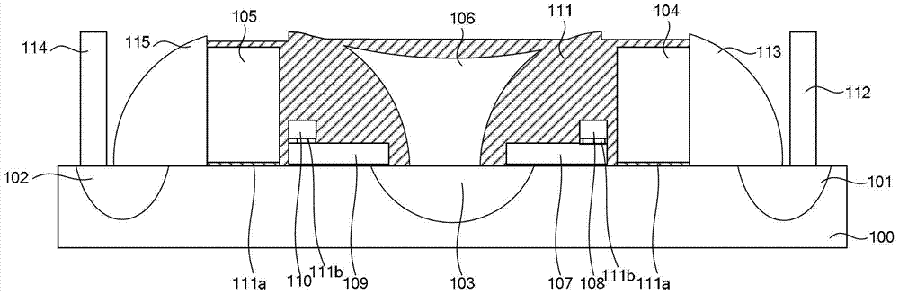
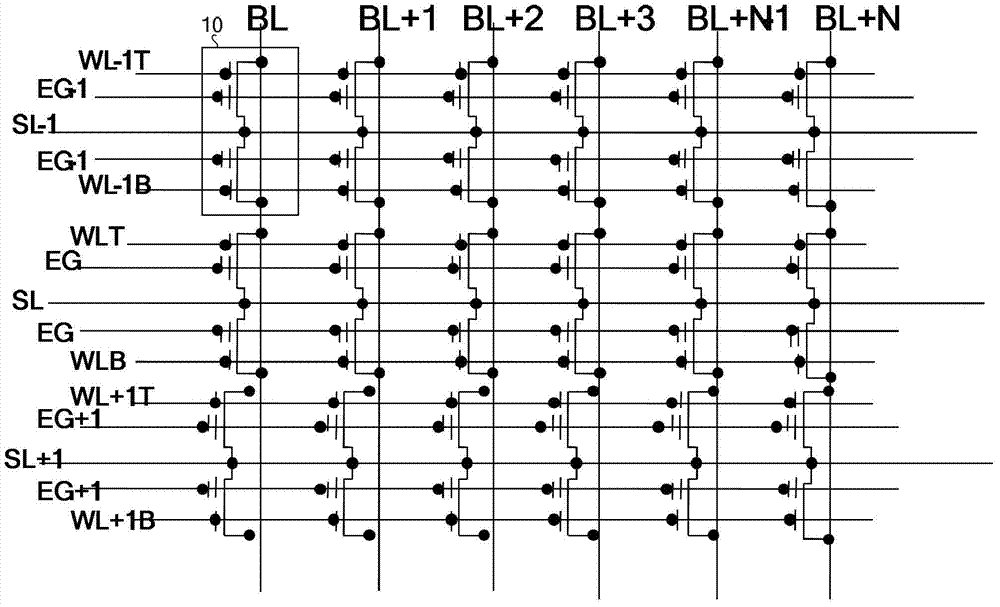
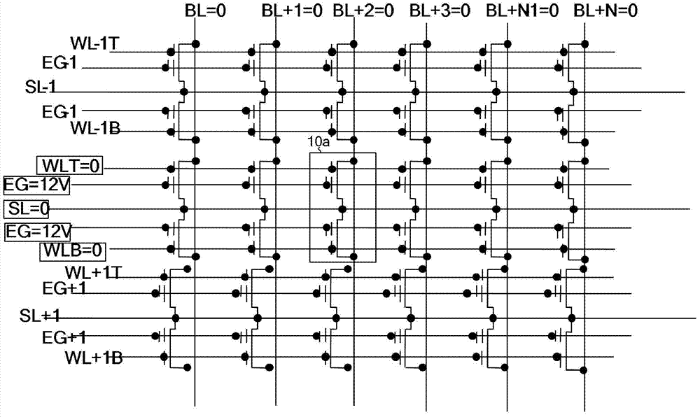
[0044] figure 1 It is a structural schematic diagram of the semiconductor memory of the present invention. Such as figure 1 As shown, the present invention provides a semiconductor memory, comprising several memory cells arranged in ar...


PUM


Abstract

The invention provides a semiconductor memory. The semiconductor memory is not provided with a control grid, wherein as a first erasure grid and a second erasure grid are respectively arranged on a first floating grid and a second floating grid, the semiconductor memory can directly conduct the erasure operation through the first erasure grid and the second erasure grid in the erasure stage, a higher erasure pressure does not need to be applied to a first bit line or a second bit line, therefore, the thickness of a word line oxidizing medium layer between the bit line and a semiconductor substrate can be reduced, the firing current is improved, the leak current can also be reduced at the same time, a lower closing current is kept, meanwhile, the reading current of the bit line is reduced during reading, so that the power consumption of the semiconductor memory is saved.

Description

technical field [0001] The invention relates to the field of semiconductor manufacturing, in particular to a semiconductor memory. Background technique [0002] Flash memory has become a research hotspot in non-volatile memory due to its convenience, high storage density, and good reliability. Since the first flash memory product came out in the 1980s, with the development of technology and the storage needs of various electronic products, flash memory has been widely used in mobile and communication devices such as mobile phones, notebooks, handheld computers and U disks. , flash memory is a kind of non-volatile memory. Its operating principle is to control the switch of the gate channel by changing the critical voltage of the transistor or memory cell to achieve the purpose of storing data, so that the data stored in the memory will not be lost due to power interruption. Disappears, and flash memory is a special structure of electrically erasable and programmable read-onl...

Claims


Application Information

Patent Timeline
Patent Type & Authority Patents(China)
IPC IPC(8): H01L27/11521H01L29/788H01L29/423G11C16/04
Inventor 顾靖
Owner SHANGHAI HUAHONG GRACE SEMICON MFG CORP
Why Eureka
Try Eureka