Semiconductor device including an insulating layer resistant to a photolithography process, electronic device, and electronic equipment

a technology of insulating layer and semiconductor, applied in the direction of semiconductor devices, solid-state devices, thermoelectric devices, etc., can solve the problem that the thickness of thin film transistors still requires further study, and achieve excellent insulating layer performance, small vth shift, and high on-off ratio

Inactive Publication Date: 2011-09-20
E INK CORPORATION
View PDF14 Cites 2 Cited by
  • Summary
  • Abstract
  • Description
  • Claims
  • Application Information

AI Technical Summary

Benefits of technology

[0008]An advantage of the present invention is to provide an organic semiconductor device of which an insulating layer is resistant to a photolithography process and characteristics are excellent (high ON-OFF ratio, small Vth shift, and small OFF-current), and an electronic device and electronic equipment that include such organic semiconductor devices and have high reliability.
[0009]A semiconductor of one aspect of the invention includes: an organic semiconductor layer made of an organic semiconductor material; a gate electrode for applying an electric field to the organic semiconductor layer; a first insulating layer insulating the gate electrode from the organic semiconductor layer; and a second insulating layer. The organic semiconductor layer is located between the first insulating layer and the second insulating layer, and the second insulating layer is composed of a polymer having fluorene skeleton.
[0010]Therefore, an organic semiconductor device having an insulating layer resistant to photolithography, and excellent characteristics (large ON-OFF ratio, small Vth shift, and small OFF-current) can be obtained.
[0011]In the semiconductor device of the aspect, a main chain of the polymer may include an oxygen atom.
[0012]The polymer including an oxygen atom can be polyester or polyether.
[0013]In the semiconductor device, the polymer may be obtained by copolymerizing a first polymerizable monomer including the fluorene skeleton, and a second polymerizable monomer including at least one of an epoxy group, an oxetane group, an acrylic acid group, and a methacrylic acid group.

Problems solved by technology

However, this thin film transistor still requires further study due to insufficient improvement of its other characteristics, especially ON-OFF ratio.

Method used


Image

  • Semiconductor device including an insulating layer resistant to a photolithography process, electronic device, and electronic equipment
  • Semiconductor device including an insulating layer resistant to a photolithography process, electronic device, and electronic equipment
  • Semiconductor device including an insulating layer resistant to a photolithography process, electronic device, and electronic equipment

Examples


example 1

1. Preparation of the Monomers

[0164]First, the following monomer compositions A to C were prepared.

Monomer composition A;

[0165]First polymerizable monomer: 4,4′-(9-fluorenylidene)bis(2-phenyloxyethylacrylate) (from Osaka Gus Chemicals, Co., Ltd.)

[0166]Second polymerizable monomer: pentaerythritol triacrylate (from Toagosei Co., Ltd., Product name: M-305)

[0167]Structural formula I / Structural formula II=20 mol % / 80 mol %

[0168]Photo polymerization initiator: Irgacure907 (from Ciba Specialty Chemicals K.K.)

[0169](Structural Formula I+Structural Formula II) / photo polymerization initiator=100 wt % / 4 wt %

Monomer Composition B;

[0170]Structural Formula I: bisphenol fluorene diglycidyl ether (from Osaka Gus Chemicals, Co., Ltd.)

[0171]Structural Formula II: dipentaerythritol hexaacrylate (from Shin-Nakamura Chemical Co., Ltd., Product name: NK Ester A-DPH)

[0172]Structural formula I / Structural formula II=50 mol % / 50 mol %

[0173]Photo polymerization initiator: Irgacure184 (from Ciba Specialty Che...

example 11

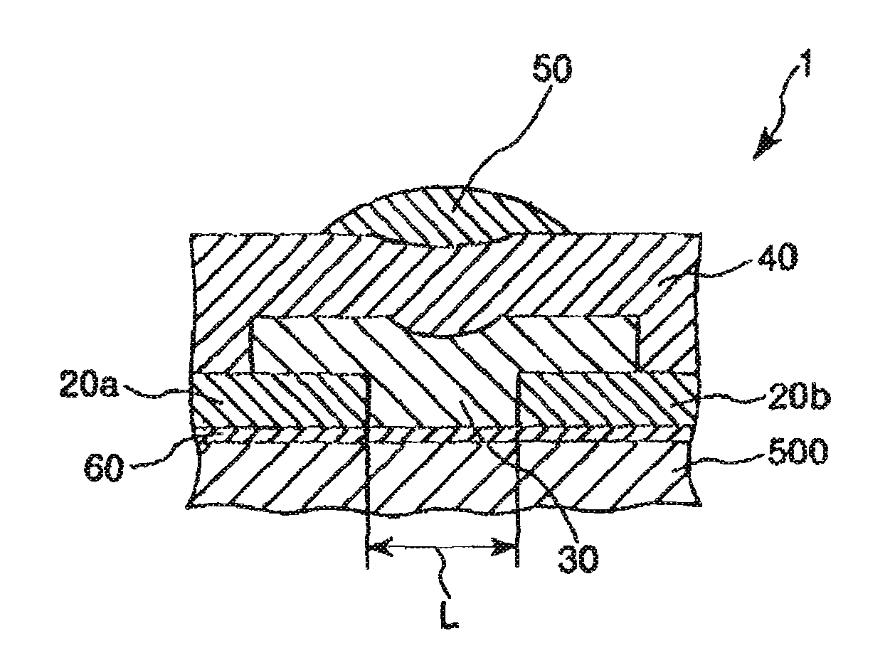
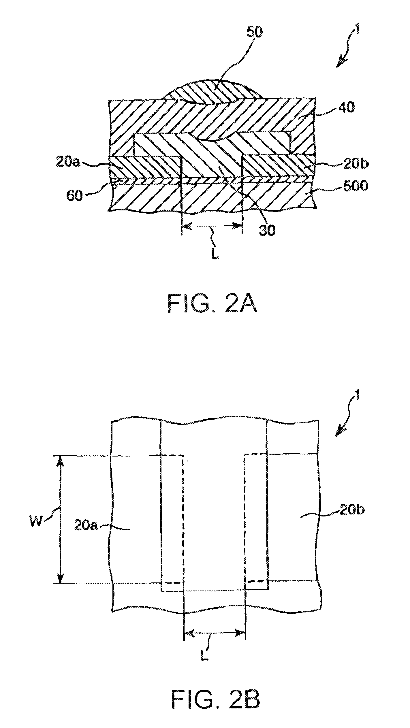
[0181]1) First, 150 μm thickness of SUS 304 substrate was prepared. Then the SUS 304 substrate was washed with water and dried.

[0182]2) A solution of the monomer composition A of which solvent is carbitol acetate and solid content was prepared to be 10 wt / vol % was applied on the substrate by spin-coating (at 1500 rpm), and then 7 mW / cm2 intensity of ultraviolet was irradiated from a direction perpendicular to the substrate for 120 seconds. Then the substrate was heated at 100 degrees Celsius for 10 minutes to effect polymerization, completing the reaction. This process provided a lower layer (second insulating layer) having an average thickness of 3 μm.

[0183]3) A gold thin film was formed on the lower layer by vapor deposition, and next a resist layer was formed thereon by photolithography. Then the gold thin film was etched by using the resist layer as a mask.

[0184]This process provided a source electrode and a drain electrode having an average thickness of 100 nm. In addition, a ...

example 12

[0193]Each thin film transistor was manufactured in the same manner as Example 11 except for using the monomer composition B as substitute for the monomer composition A.


PUM

PropertyMeasurementUnit
thicknessaaaaaaaaaa
mol %aaaaaaaaaa
thicknessaaaaaaaaaa

Abstract

A semiconductor device includes: an organic semiconductor layer made of an organic semiconductor material; a gate electrode for applying an electric field to the organic semiconductor layer; a first insulating layer insulating the gate electrode from the organic semiconductor layer; and a second insulating layer. The organic semiconductor layer is located between the first insulating layer and the second insulating layer, and the second insulating layer is composed of a polymer having a fluorene skeleton.

Description

BACKGROUND[0001]1. Technical Field[0002]The present invention relates to a semiconductor device, an electronic device, and electronic equipment.[0003]2. Related Art[0004]The development of thin film transistors (organic semiconductor devices) using organic materials (organic semiconductor materials) that exhibit semiconducting electrical conductivity has been recently progressed.[0005]These thin film transistors have advantages such as suitability for being thinned and lightened, flexibility, low material costs, and so forth, so as to be expected as a switching element of a flexible display and so forth.[0006]Such thin film transistors include a transistor disclosed in JP-A-2005-101555, for example. The transistor has such structure that an insulating layer including aromatic compound and / or aromatic ring containing polymer is formed on an organic semiconductor layer at an opposite side to a gate insulating layer for an improvement of carrier mobility.[0007]However, this thin film t...

Claims


Application Information

Patent Timeline
Patent Type & Authority Patents(United States)
IPC IPC(8): H01L29/08
CPCH01L51/0043H01L51/0541H01L51/0035H01L51/0036H01L51/0039H01L51/006H01L51/052H01L51/0562H10K85/115H10K85/113H10K85/111H10K85/151H10K85/633H10K10/471H10K10/486H10K10/464
Inventor YAMAMOTO, HITOSHI
Owner E INK CORPORATION
Why Eureka
Try Eureka