Method of manufacturing high-k gate dielectric by use of annealing in high-pressure hydrogen atmosphere

Inactive Publication Date: 2005-07-05
POONGSAN MICROTEC
View PDF5 Cites 54 Cited by
  • Summary
  • Abstract
  • Description
  • Claims
  • Application Information

AI Technical Summary

Benefits of technology

[0010]Therefore, it is an object of the present invention to alleviate the problems in the related art and to provide a method of effective

Problems solved by technology

First, although the high-temperature annealing process using forming gas, which is applied for the high-k gate dielectric before the metallization, can passivate interface/fixed charges, it leads to increased effective thickness of the dielectric, and deteriorated leakage current properties due to crystallization. Hence, this process should be perfor

Method used


Image

  • Method of manufacturing high-k gate dielectric by use of annealing in high-pressure hydrogen atmosphere
  • Method of manufacturing high-k gate dielectric by use of annealing in high-pressure hydrogen atmosphere
  • Method of manufacturing high-k gate dielectric by use of annealing in high-pressure hydrogen atmosphere

Examples


example 1

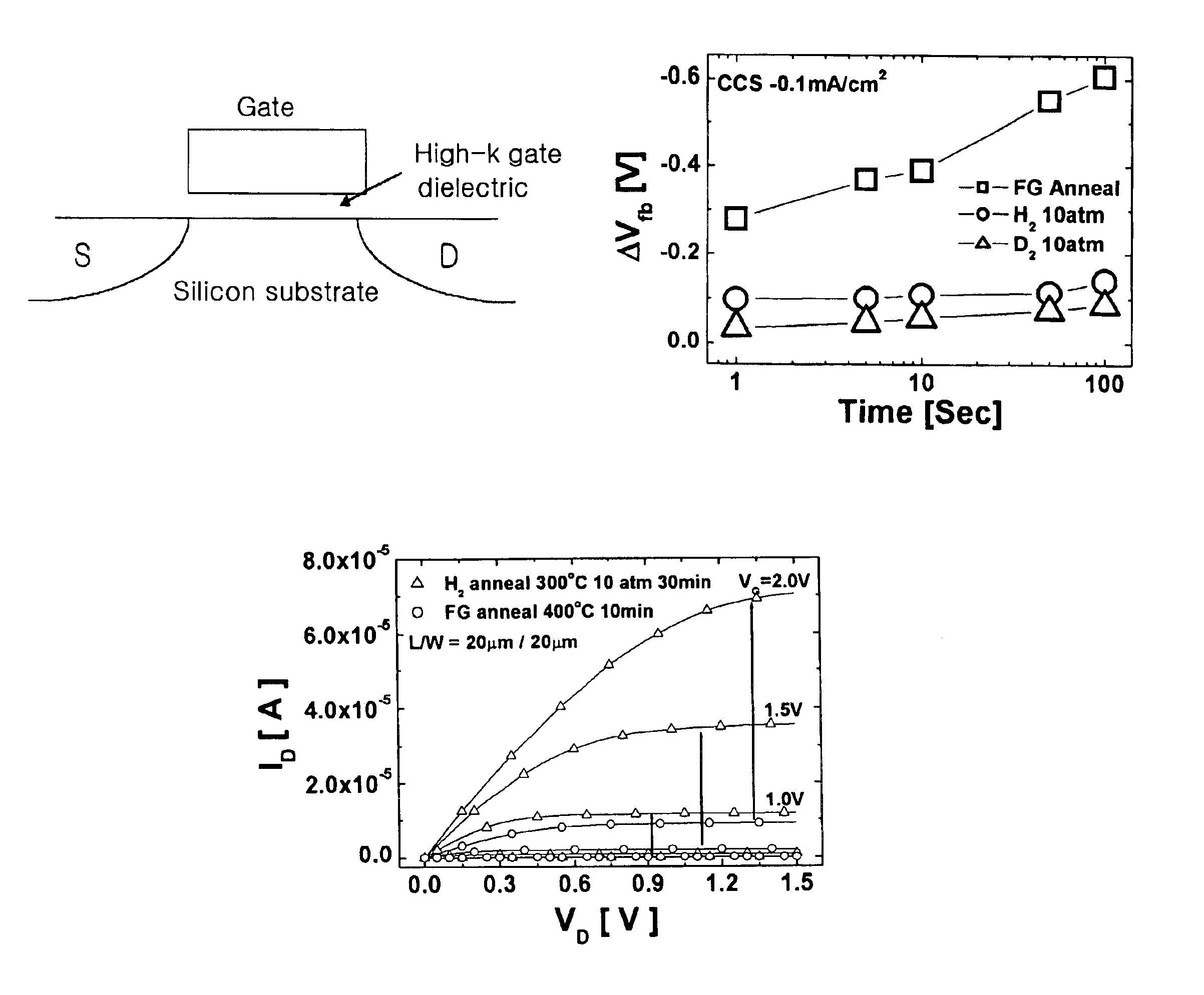
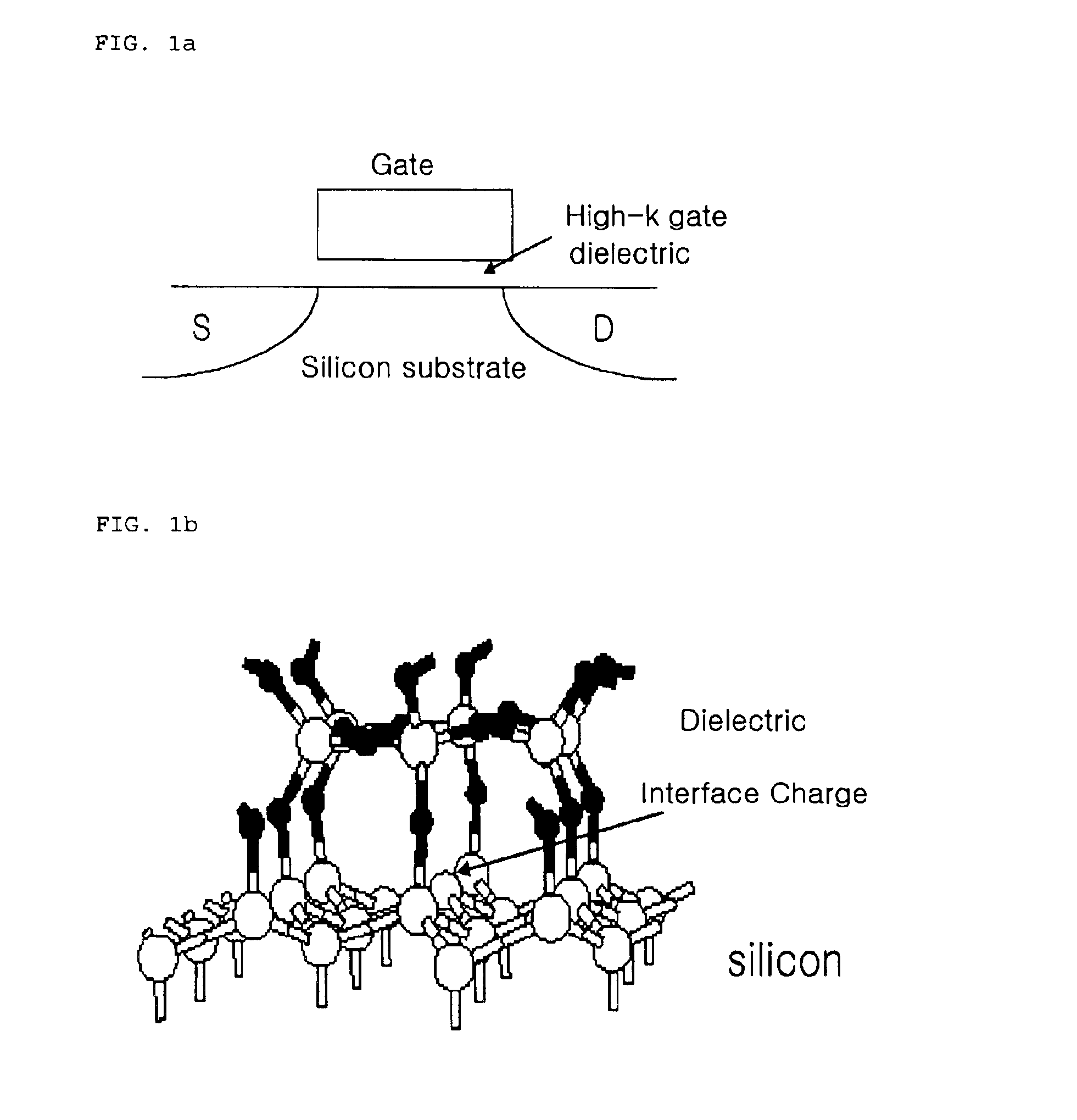
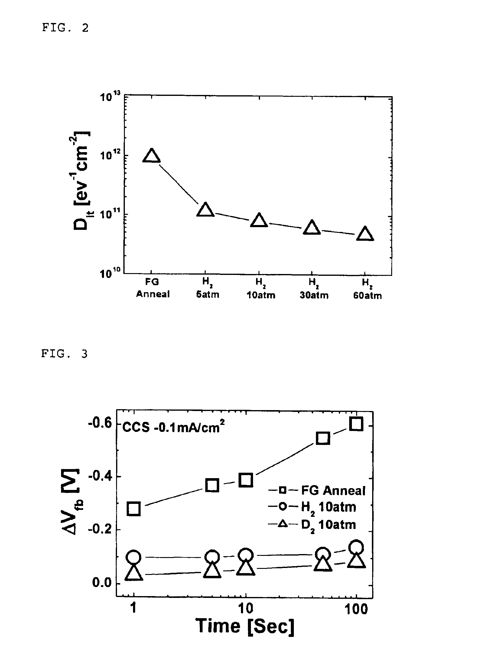
[0034]A hafnium oxide (HfO2) gate dielectric was formed by means of an atomic layer deposition (ALD), and was then subjected up to metallization, to manufacture a MOSFET device. Subsequently, the manufactured device sample was placed into a sealed container, and annealed at 400° C. under 50 atm for 30 min in a 100% hydrogen or deuterium atmosphere. The thus annealed sample was compared to one subjected to conventional annealing process (at 400° C. under 1 atm for 30 min in a 4% hydrogen atmosphere). The results are as follows.

[0035](1) The hydrogen concentration contained in the gate dielectric was confirmed to be increased by about 10-100 times by means of SIMS.

[0036](2) The interface state density and fixed charge density of the device sample annealed according to the present invention were about 5×10¹⁰ / cm2-eV similar to those of silica devices, which corresponded to a value reduced by about {fraction (1 / 20)} or less, compared to about 1012 / cm2-eV of the device sample annealed con...


PUM


Abstract

Disclosed is a method of manufacturing a high-k gate dielectric, characterized in that an annealing process in a forming gas atmosphere, corresponding to a final step of a manufacturing process of a semiconductor device based on MOSFET fabrication techniques, is applied for a high-k gate dielectric-containing semiconductor device, under high pressure, instead of conventional atmospheric pressure, whereby passivation effects of interface charges and fixed charges of the semiconductor device can be maximized even at relatively low temperatures.

Description

BACKGROUND OF THE INVENTION[0001]1. Field of the Invention[0002]The present invention relates to a method of manufacturing a high-k gate dielectric, characterized in that an annealing process in a forming gas atmosphere, corresponding to a final step of a manufacturing process of a semiconductor device based on fabrication techniques of MOSFET (Metal-Oxide-Silicon Field Effect Transistor), is applied for a semiconductor device having a high-k gate dielectric, under conditions of high concentration (100%) and high pressure, instead of conventional conditions of low concentration (3-5%) and atmospheric pressure, whereby interface charges and fixed charges of the semiconductor device can be maximally passivated even at relatively low temperatures.[0003]2. Description of the Related Art[0004]In general, a manufacturing method of a semiconductor device, which uses silica (SiO2) as a gate dielectric, includes metallization, followed by annealing at about 400450° C. for 10-30 min in a form...

Claims


Application Information

Patent Timeline
IPC IPC(8): H01L21/30H01L21/02H01L21/28H01L29/51H01L21/314H01L29/40H01L21/31
CPCH01L21/28176H01L21/28194H01L21/3003H01L29/517H01L21/3141H01L29/51H01L21/02178H01L21/02337H01L21/31
Inventor HWANG, HYUN SANG
Owner POONGSAN MICROTEC
Why Eureka
Try Eureka