
Semiconductor device and method of manufacturing the same

a technology of semiconductor devices and semiconductors, applied in semiconductor devices, semiconductor/solid-state device details, capacitors, etc., can solve the problems of complex structure and damage to the underlying ferroelectric film, and achieve the effect of suppressing the damage to the capacitor formed and simplifying the respective wiring connection structur

Inactive Publication Date: 2005-07-05
FUJITSU SEMICON LTD
View PDF12 Cites 10 Cited by
  • Summary
  • Abstract
  • Description
  • Claims
  • Application Information

AI Technical Summary

Benefits of technology

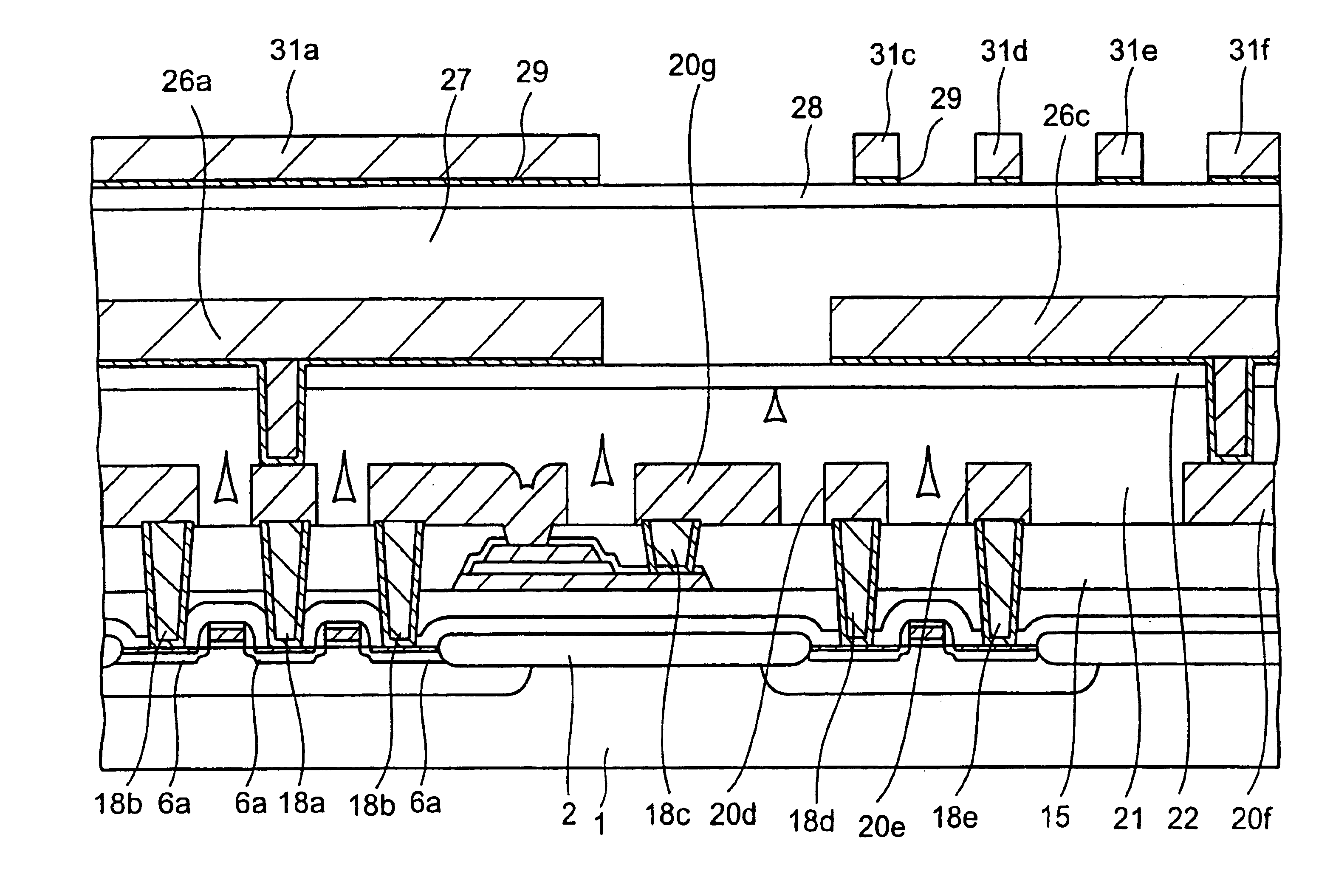
[0018]It is an object of the present invention to provide a semiconductor device capable of simplifying respective wiring connection structures to an upper electrode and a lower electrode of a capacitor by suppressing the damage to the capacitor formed over a transistor, and a method of manufacturing the same.
[0019]According to the above invention, the contact holes on the upper electrode of the capacitor and the contact holes on the lower electrode are not simultaneously opened, but the hole on the lower electrode is formed simultaneously with the holes on the impurity diffusion layers and then plugs are buried in the holes and then the hole is solely formed on the upper electrode of the capacitor. Therefore, the degradation of the dielectric film caused when the hole is formed on the upper electrode can be suppressed and the capacitor characteristics can be held satisfactorily.
[0020]In addition, since all holes can be formed in the second insulating film covering the capacitor by two steps, the increase in steps can be prevented.

Problems solved by technology

Thus, the structure becomes complicated and thus a number of manufacturing steps are requested.
Therefore, if it is attempted to form simultaneously these holes, there is such a possibility that, because the hole formed on the upper electrode is formed early, the underlying ferroelectric film is damaged.

Method used


Image

  • Semiconductor device and method of manufacturing the same
  • Semiconductor device and method of manufacturing the same
  • Semiconductor device and method of manufacturing the same

Examples


Embodiment Construction

[0033]An embodiment of the present invention will be explained in detail with reference to the accompanying drawings hereinafter.

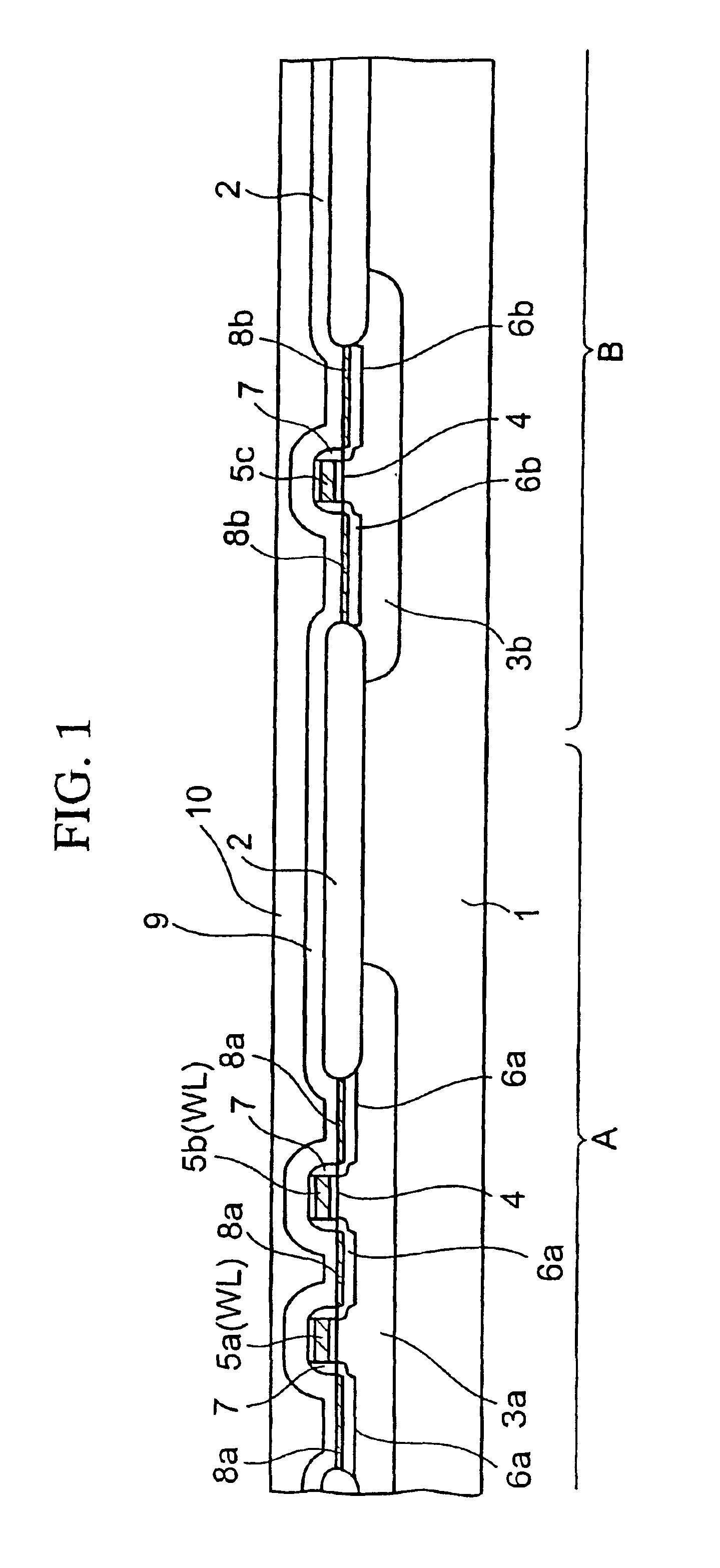
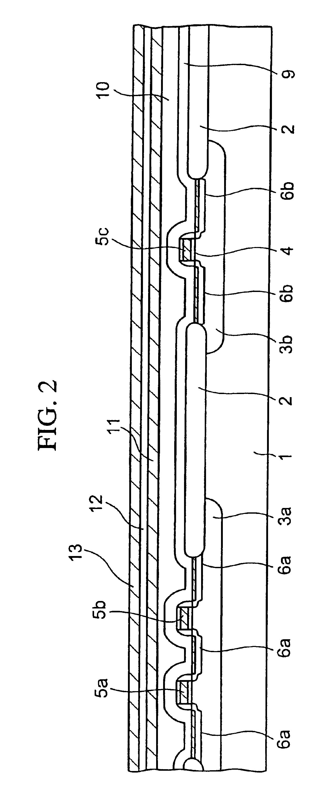
[0034]FIG. 1 to FIG. 21 are sectional views showing a semiconductor device manufacturing method in order of steps according to an embodiment of the present invention.

[0035]First, steps required to get the sectional structure shown in FIG. 1 will be explained hereunder.

[0036]As shown in FIG. 1, a device isolation insulating film 2 is formed on a surface of an n-type or p-type silicon (semiconductor) substrate 1 by the LOCOS (Local Oxidation of Silicon) method. The STI (Shallow Trench Isolation) method, etc. in addition to the LOCOS method may be employed to form the device isolation insulating film 2.

[0037]After such device isolation insulating film 2 is formed, a p-well 3a and an n-well 3b are formed by introducing selectively the p-type impurity and the n-type impurity into predetermined active regions (transistor forming regions) in a memory cell region ...


PUM


Abstract

A semiconductor device formed by forming contact holes in the insulating film, that covers the source / drain of the MOSFET and the capacitor in the memory cell region, on the lower electrode of the capacitor by the same steps, then filling the plugs into contact holes, and then forming the contact hole on the upper electrode of the capacitor. Accordingly, there can be provided the semiconductor device having the ferroelectric capacitor, capable of simplifying respective wiring connection structures to the upper electrode and the lower electrode of the capacitor by suppressing the damage to the capacitor formed over the transistor.

Description

[0001]This application is a division of prior application Ser. No. 09 / 750,069 filed Dec. 29, 2000 now U.S. Pat. No. 6,509,593.BACKGROUND OF THE INVENTION[0002]1. Field of the Invention[0003]The present invention relates to a semiconductor device and to a method of manufacturing the same and, more particularly, to a semiconductor device including a capacitor having a ferroelectric layer or a high-dielectric layer and to a method of manufacturing the same.[0004]2. Description of the Related Art[0005]The flash memory, the ferroelectric memory (FeRAM), etc. are known, as the nonvolatile memory that can still store the information after the power supply is turned off.[0006]The flash memory has such a structure that the information are stored by accumulating charges in the floating gate that is buried in the gate insulating film of the insulated-gate field effect transistor (IGFET). The tunnel current that passes through the insulating film formed between the floating gate and the semicon...

Claims


Application Information

Patent Timeline
Patent Type & Authority Patents(United States)
IPC IPC(8): H01L27/115H01L21/70H01L21/768H01L21/8246H01L21/02H01L23/522H10B12/00H10B20/00H10B69/00
CPCH01L21/76802H01L21/7682H01L21/76829H01L27/11502H01L27/11507H01L28/55H01L2924/0002H01L2924/00H01L21/76885H01L23/5223H10B53/30H10B53/00H01L27/105
Inventor INOUE, KENICHIOBATA, YOSHINORISAITO, TAKEYASUSAIGOH, KAORUSASHIDA, NAOYATANI, KOJIMIURA, JIROUYOKOTA, TATSUYAMIHARA, SATORUHIKOSAKA, YUKINOBUOZAKI, YASUTAKA
Owner FUJITSU SEMICON LTD
Learn More