Nonvolatile semiconductor storage device

Inactive Publication Date: 2005-07-05
SONY SEMICON SOLUTIONS CORP
View PDF3 Cites 3 Cited by
  • Summary
  • Abstract
  • Description
  • Claims
  • Application Information

AI Technical Summary

Benefits of technology

[0007]It is therefore an object of the present invention to provide a nonvolatile semiconducto

Problems solved by technology

However, the existing method of securing the design margin entails a drawback well known to those active in the field, in that rest

Method used


Image

  • Nonvolatile semiconductor storage device
  • Nonvolatile semiconductor storage device
  • Nonvolatile semiconductor storage device

Examples


first embodiment

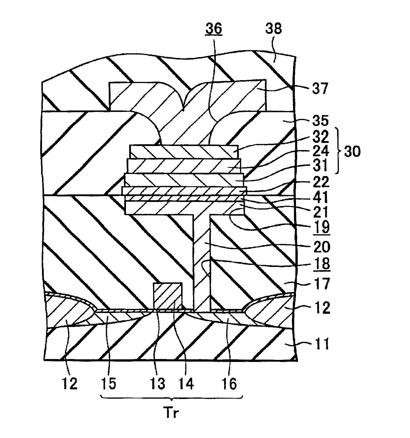
[0026]A nonvolatile semiconductor storage device according to a first embodiment of the present invention will now be explained with reference to a schematic cross-sectional view of FIG. 1.

[0027]As shown in FIG. 1, an element isolation oxide film 12 separating an element forming region is formed on a semiconductor substrate 11 (e.g., p-type silicon substrate). On the element forming region of the semiconductor substrate 11 is formed a gate insulating film 13 comprising a silicon oxide film of 1.5 nm thick, for example, and a silicon nitride film of 2 nm thick, for example.

[0028]On the above-mentioned gate insulating film 13 is formed a gate electrode 14. Further, a source region 15 is formed on one side of the gate electrode 14 on the semiconductor substrate 11, while a drain region 16 is formed on the other side thereof on the semiconductor substrate 11. A transistor Tr is constructed in this manner.

[0029]On the substrate 11, a first interlayer insulating film 17 covering the trans...

second embodiment

[0054]Now, referring to a schematic cross-sectional view of FIG. 3, a modified nonvolatile semiconductor storage device according to a second embodiment will be described with an explanation of a nonvolatile semiconductor storage device using Bi3TiNbO9 as the ferroelectric material of a capacitor.

[0055]As shown in FIG. 3, an element isolation oxide film 12 separating an element forming region is formed on a semiconductor substrate 11 (e.g., p-type silicon substrate). In the element forming region of the semiconductor substrate 11 is formed a gate insulating film 13 comprising a silicon oxide film of a thickness of 1.5 nm, for example, and a silicon nitride film of a thickness of 2 nm, for example.

[0056]A gate electrode 14 is formed on the gate insulating film 13. In addition, a source region 15 is formed on one side of a gate electrode 14 on the semiconductor substrate 11, while a drain region 16 is formed on the other side thereof on the semiconductor substrate 11. A transistor Tr ...

third embodiment

[0080]Now, referring to a schematic section of FIG. 5, another modified nonvolatile semiconductor storage device according to a third embodiment will be described with an explanation of a nonvolatile semiconductor storage device employing a complex capacitor structure.

[0081]As depicted in FIG. 5, an element isolation oxide film 12 separating the element forming region is formed on a semiconductor substrate 11 (e.g., p-type silicon substrate). In the element forming region of the semiconductor substrate 11 is formed a gate insulating film 13 comprised of a silicon oxide film of 1.5 nm thick, for example, and a silicon nitride film of 2 nm thick, for example.

[0082]A gate electrode 14 is formed on the gate insulating film 13, and a source region 15 is formed on one side of the gate electrode 14 on the semiconductor substrate 11, while a drain region 16 is formed on the other side thereof on the semiconductor substrate 11. A transistor Tr is constructed in this manner.

[0083]On the semic...


PUM


Abstract

In order to provide a nonvolatile semiconductor storage device designed to take off such existing restraint on the degree of freedom of device design as needed for the purpose of securing design margin, thus realizing a ferroelectric, nonvolatile storage device of high integration density, there is disclosed a capacitor using a ferroelectric thin film is provided, so that the apparent coercive electric field value in the operational guaranteed margin temperature of the nonvolatile semiconductor storage device when regarded as the voltage applied to the capacitor remains within the range of design margin of the nonvolatile semiconductor storage device at the coercive electric field value at the specified temperature, in which a metal oxide of a layer structure having the ferroelectric-to-normal dielectric phase transition point of 800° C. or higher may be used for the ferroelectric thin film.

Description

RELATED APPLICATION DATA[0001]The present application claims priority to Japanese Application P2000-110139 filed Apr. 12, 2000, which application is incorporated herein by reference to the extent permitted by law.BACKGROUND OF INVENTION[0002]1. Field of the Invention[0003]This invention relates to a nonvolatile semiconductor storage device, and more particularly, to a nonvolatile semiconductor storage device using a ferroelectric thin film.[0004]2. Description of the Related Art[0005]Various proposals and suggestions regarding the construction of nonvolatile semiconductor storage devices of high integration density in terms of use of ferroelectric thin films for semiconductor storage elements are known. In the currently available technology for designing or fabricating such nonvolatile storage devices, the quantity of change in the residual spontaneous polarization of the ferroelectric thin film within the operational guaranteed temperature of the coercive electric field serves as o...

Claims


Application Information

Patent Timeline
IPC IPC(8): H01L21/02H01L21/316H01L21/285H01L21/8242H01L27/108H01L27/10
CPCH01L21/31691H01L28/55H01L21/28568H01L28/75H01L21/02197
Inventor TANAKA, MASAHIRO
Owner SONY SEMICON SOLUTIONS CORP
Why Eureka
Try Eureka