Light emitting device, driving method for the same and electronic apparatus

a technology of light-emitting devices and electronic devices, applied in the field of oled panels, can solve the problems of oled organic light-emitting layers deteriorating at a different rate, oled brightness falling, and oled brightness lowering

Inactive Publication Date: 2005-07-05
SEMICON ENERGY LAB CO LTD
View PDF52 Cites 64 Cited by
  • Summary
  • Abstract
  • Description
  • Claims
  • Application Information

AI Technical Summary

Benefits of technology

[0015]The present inventor has paid attentions to the fact that the lowering in OLED brightness due to deterioration is less when light is emitted while keeping the current flowing through the OLED at constant rather than when light is emitted while keeping the OLED drive voltage at constant. Note that, in the description, the current flowing through an OLED is referred to as an OLED drive current (Iel). It has been considered that the OLED brightness change due to OLED deterioration can be prevented due to control of the OLED brightness not by a voltage but by a current.
[0019]The present invention can suppress the lowering in OLED brightness by the above configuration even where an organic light-emitting layer deteriorates. As a result, a clear image can be displayed. Meanwhile, in the case of a color-display light-emitting device using OLEDs corresponding to respective colors, if the OLED organic light-emitting layer deteriorates at a rate different between the colors prevents the colors from being unbalanced in brightness, thereby displaying a desired color.
[0020]Meanwhile, even where the temperature of the organic light-emitting layer is influenced by outside-air temperature or the heat generated by the OLED panel itself, the OLED current can be controlled to a desired value. Accordingly, because the OLED drive current and the OLED brightness are in proportion, the OLED brightness can be suppressed from changing. Furthermore, consumption current can be prevented from increasing due to temperature rise. In the case of a color-display light-emitting device, the colors are suppressed from changing in OLED brightness without being affected by temperature change. Accordingly, the colors can be prevented from being unbalanced in brightness thereby displaying a desired color.
[0021]Furthermore, because generally the change rate of OLED drive current due to temperature change is different depending on the kind of an organic light-emitting material, there is a possibility that the colors in color display variously change in OLED brightness depending on temperature. However, the light-emitting device of the present invention can obtain a desired brightness without being affected by temperature change. Accordingly, the colors are prevented from being unbalanced in brightness thus displaying a desired color.
[0022]Meanwhile, the general light-emitting device has an electric resistance on the wiring to supply current to each pixel, and hence the potential thereon somewhat drops due to wiring length. The potential drop largely differs depending on an image to be displayed. Particularly, in a plurality of pixels to be supplied by a current from the same wiring, where the ratio of the pixels having many gray scales increases, the current flowing the wiring increases to conspicuously cause potential drop. The potential drop decreases the voltage to be applied to the OLED of each pixel, hence decreasing the current to be supplied to the pixel. Accordingly, in the case to provide display in a constant gray scale on a certain predetermined pixel, when there is change in gray scale on another pixel being supplied with current through the same wiring, this causes a change in the current to be supplied to the predetermined pixel, resultingly changing the gray scale. However, the light-emitting device of the present invention can obtain a measurement value and reference value on each display image thereby correcting the OLED current. Accordingly, even where there is change in a display image, it can be displayed at a desired gray scale by the correction.

Problems solved by technology

It is problematic in placing the light-emitting device into practical application that the brightness of an OLED lowers due to deterioration in the organic light-emitting material.
This results in obscured image display.
Consequently, there is a possibility that the OLED organic light-emitting layer deteriorates at a different rate dependently upon the color.
In this case, as time elapses the brightness of OLED becomes different by the color, making impossible for the light-emitting device to display an image with a desired color.
In this manner, because OLED brightness varies with the temperature of the organic light-emitting layer, display is difficult at a desired gray scale.
The consumption current of the light-emitting device increases with the rise of temperature.
The brightness balance, if disordered between the colors, makes impossible to display in a desired color.

Method used


Image

  • Light emitting device, driving method for the same and electronic apparatus
  • Light emitting device, driving method for the same and electronic apparatus
  • Light emitting device, driving method for the same and electronic apparatus

Examples


embodiment mode 1

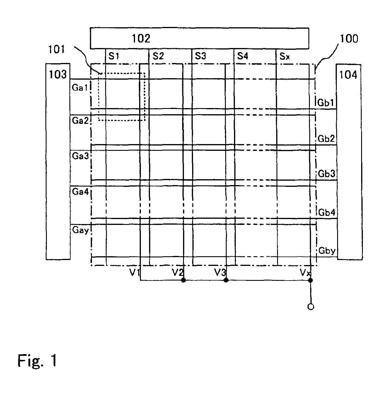
[0052]FIG. 1 shows a block diagram of an OLED panel structure of the present invention. 100 is a pixel section forming a plurality of pixels 101 in a matrix form. Meanwhile, 102 is a signal line drive circuit, 103 is a first scanning line drive circuit and 104 is a second scanning line drive circuit.

[0053]In FIG. 1, although the signal line drive circuit 102, the first scanning line drive circuit 103 and the second scanning line drive circuit 104 are formed on the same substrate as the pixel section 100, the present invention is not limited to that structure. The signal line drive circuit 102, the first scanning line drive circuit 103 and the second scanning line drive circuit 104 may be formed on a different substrate from the pixel section 100 and connected to the pixel section 100 through an FPC or the like. Meanwhile, in FIG. 1, although the signal line drive circuit 102, the first scanning line drive circuit 103 and the second scanning line drive circuit 104 are provided one pe...

embodiment mode 2

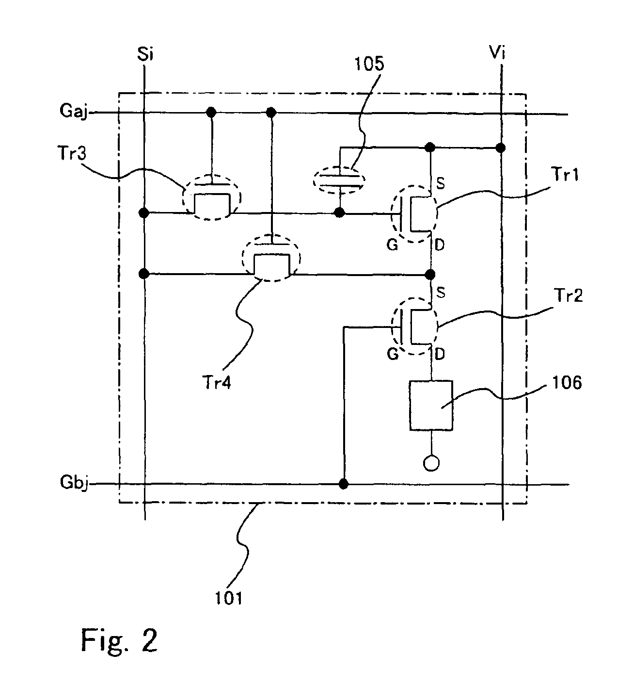
[0067]Now, explanation will be made on the drive to the light-emitting device shown in FIG. 2, using FIG. 3. In the present embodiment mode, the operation of each pixel of the light-emitting device shown in FIG. 2 is explained by separating with a write period Ta and a display period Td.

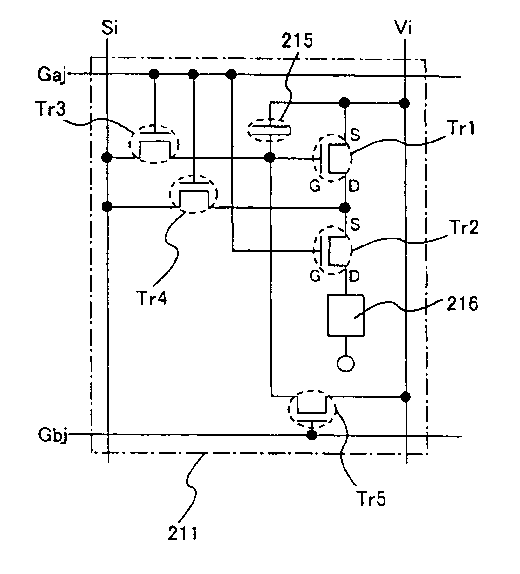
[0068]In the write period Ta, the first scanning line Gaj is selected. When the first canning line Gaj is selected, the transistors Tr3 and Tr4 connected at their gate electrode to the first scanning line Gaj turn on. Note that, in the write period Ta, the second scanning line Gbj is not selected and hence the Tr2 is off.

[0069]On the basis of a potential of a video signal inputted to the signal line drive circuit 102, constant currents Ic flow respectively between the signal lines S1-Sx and the power lines V1-Vx. Note that, in the description, the current Ic is referred to as a signal current.

[0070]FIG. 3A shows a schematic diagram of the pixel 101 that, in the write period Ta, a constant current Ic ...

embodiment mode 3

[0091]This embodiment mode explains an embodiment mode different from Embodiment Mode 2 of driving the light-emitting device of FIG. 2, using FIG. 6. In this embodiment mode, the operation of each pixel of the light-emitting device of FIG. 2 will be explained by separating with a write period Ta, a display period Td and a non-display period Te. Note that, because the operation on the pixel in the write period Ta and display period Td has already been explained in Embodiment Mode 2, explanation will be herein made on the operation on the pixel in a non-display period Te.

[0092]The non-display period Te occurs after terminating a display period Td and before an occurrence of a display period Td. In the non-display period Td, the first scanning line Gaj and the second scanning line Gbj are not selected.

[0093]FIG. 6 shows a schematic diagram of the pixel in a non-display period Te. The transistor Tr3 and the transistor Tr4 are off. Meanwhile, the transistor Tr2 is also off. Accordingly, ...


PUM


Abstract

It is a problem to provide a light-emitting device capable of obtaining a constant brightness without being affected by deterioration in an organic light-emitting layer or temperature change, and of making desired color display. The lowering in OLED brightness due to deterioration is reduced by causing the OLED to emit light while keeping constant the current flowing through the OLED instead of causing the OLED to emit light while keeping constant the OLED drive voltage. Namely, OLED brightness is controlled not by voltage but by current thereby preventing against the change in OLED brightness due to deterioration of OLED. Specifically, the drain current Id of a transistor for supplying a current to the OLED is controlled in a signal line drive circuit thereby keeping constant the drain current Id without relying upon the value of a load resistance.

Description

CROSS-REFERENCE TO RELATED APPLICATIONS[0001]This application is a divisional (and claims the benefit of priority under 35 USC 120) of U.S. application Ser. No. 10 / 101,628, filed Mar. 21, 2002, now U.S. Pat. No. 6,661,180, which, under 35 USC 119, claims the benefit of a foreign priority application filed in Japan as Ser. No. 2001-081779 on Mar. 22, 2001. This application claims priority to both of these applications, and both of these applications are incorporated by reference.BACKGROUND OF THE INVENTION[0002]1. Field of the Invention[0003]The present invention relates to an OLED panel having an organic OLED (OLED: Organic Light Emitting Diode) formed on a substrate and sealed between the substrate and a cover member, and also to an OLED module mounting an IC or the like including a controller on such an OLED panel. In the present description, both an OLED panel and an OLED module are, collectively, referred to as a light-emitting device. The present invention, furthermore, relates...

Claims


Application Information

Patent Timeline
Patent Type & Authority Patents(United States)
IPC IPC(8): G09G3/32G09G3/20H01L27/32H01L29/08
CPCG09G3/3225G09G3/325G09G3/3266G09G3/3275G09G3/3283G09G3/3291H01L27/3276H01L27/1255G09G3/2022G09G2300/0426G09G2300/0465G09G2300/0842G09G2300/0861G09G2300/0895G09G2310/0251G09G2310/0262G09G2310/027G09G2310/08G09G2320/0233G09G2320/0266G09G2320/041G09G2320/043H01L27/3244H01L29/4908H10K59/12H10K59/131
Inventor KOYAMA, JUN
Owner SEMICON ENERGY LAB CO LTD
Why Eureka
Try Eureka