Electro-optic modulators

a modulator and optical technology, applied in the field of modulation or variable attenuation of optical radiation, can solve the problems of modulation device disadvantageously limited optical bandwidth, inability to readily couple input and output waveguides, and light intensity modulation exiting dielectric waveguides

Inactive Publication Date: 2005-07-05
UNIVERSITY OF OTTAWA
View PDF28 Cites 23 Cited by
  • Summary
  • Abstract
  • Description
  • Claims
  • Application Information

AI Technical Summary

Benefits of technology

[0010]The present invention seeks to eliminate, or at least mitigate, one or more of the disadvantages or limitations of known modulators or at least provide an alternative and, to this end, provides a plasmon-polariton modulation means of the kind disclosed in International patent applications Nos. WO 01/48521 and WO 03/001258, characterized in that the surrounding material comprises first and second distinct portions with the strip extending between them and at least one electrode is positioned adjacent the strip, at least the f

Problems solved by technology

This results in a modulation in the intensity of the light exiting the dielectric waveguide.
These known modulation devices disadvantageously have limited optical bandwidth and, in the case of the ATR devices, are not readily coupled to inpu

Method used


Image

  • Electro-optic modulators
  • Electro-optic modulators
  • Electro-optic modulators

Examples


first embodiment

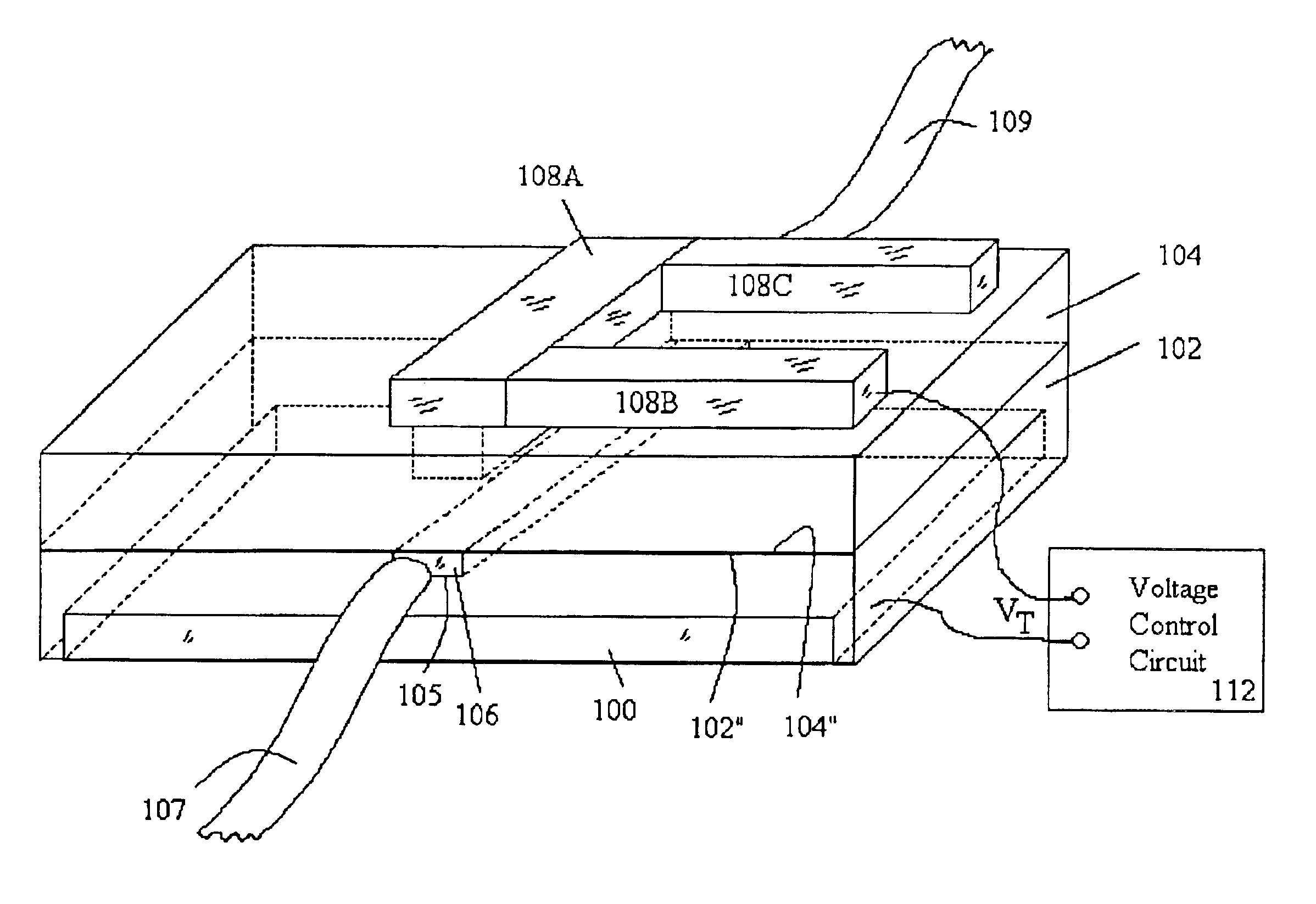
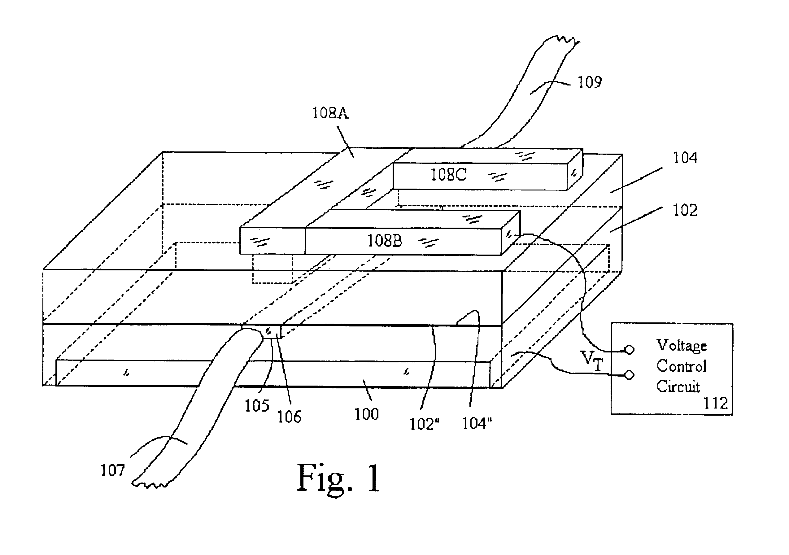
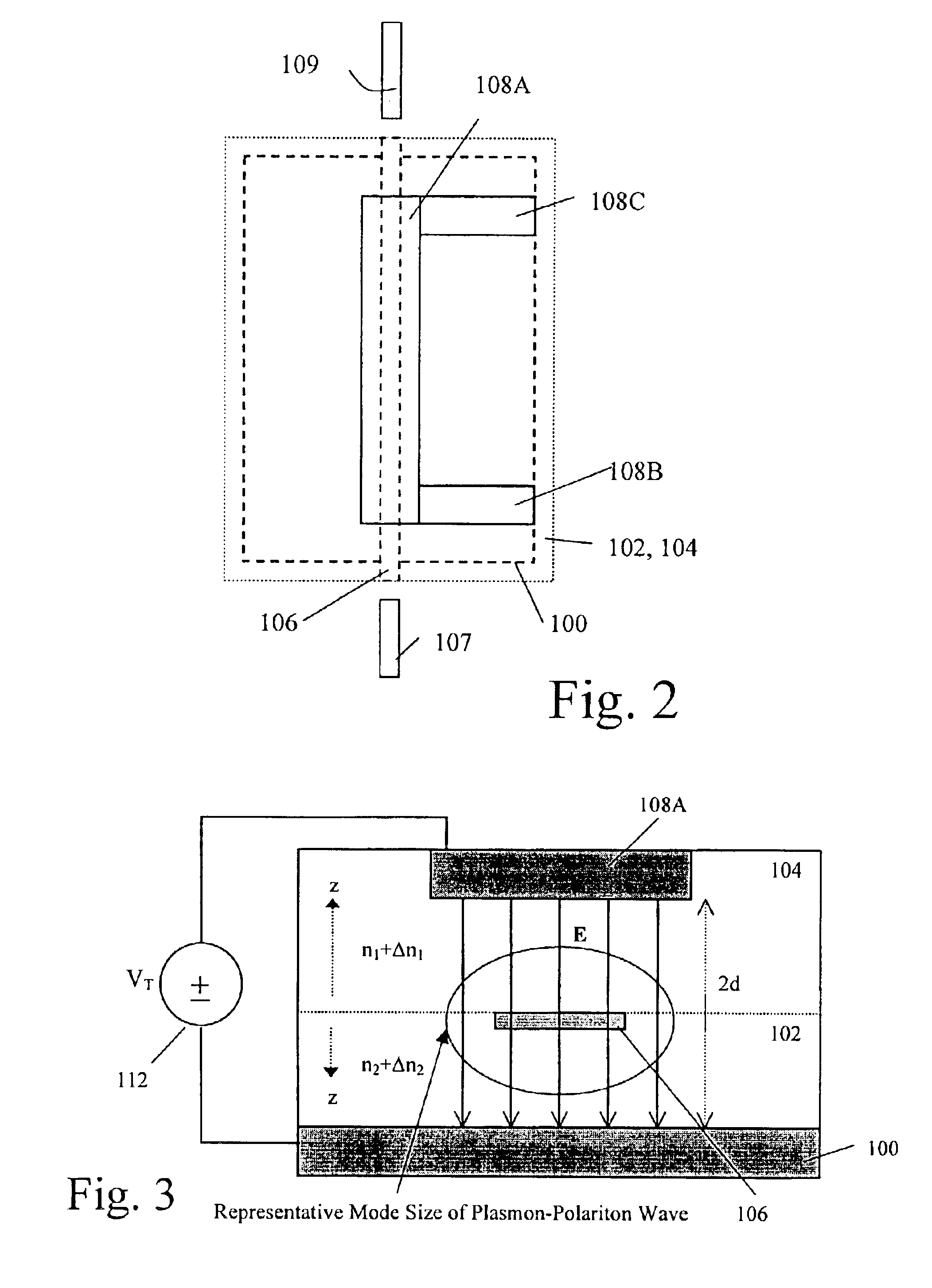
[0039]the invention, the modulator illustrated in FIGS. 1, 2 and 3, comprises a die formed by two wafer portions of electro-optic material 102 and 104 having respective opposed flat surfaces 102″ and 104″ wafer-bonded together. A thin metal waveguide strip 106 deposited in a trench 105 formed (e.g. etched) in the surface 102″ extends the length of the die. Opposite ends of strip 106 are coupled to input and output waveguides 107 and 109, e.g., optical fiber waveguides, waveguides in an integrated optics device, or other plasmon polariton waveguides. The input waveguide is arranged such that the substantially TM polarized plasmon-polariton wave is excited efficiently. For example, the waveguide 107 could be a polarization-maintaining fiber connecting a polarized light source to the strip 106 with appropriate orientation. Alternatively, the input waveguide 107 could be the output plasmon-polariton waveguide of the external cavity laser disclosed in copending U.S. Provisional patent ap...

second embodiment

[0064]Because the strip 106 is a conductor, it too can be used as an electrode. Thus, FIGS. 6, 7 and 8 illustrate a second embodiment in which the operating voltage is applied between strip 106 and external electrodes 100a and 108 on the outermost surface of the electro-optic wafer portions 102 and 104, respectively. A plurality of optically non-invasive branch connector elements 114, similar in width and thickness to waveguide strip 106, spaced at intervals along the length of the waveguide strip 106 extend laterally from one side of the waveguide strip 106 to a parallel via 116 which is filled and capped with an electrode pad 118 so that electrical contact can be made to the waveguide 106 from the top of the modulator die. It should be noted that electrode pad 118 does not overlie the strip 106, and is positioned sufficiently far away from the strip 106 so as to not interact with the plasmon-polariton wave propagating along the strip 106.

[0065]FIG. 7 shows connecting electrodes 12...

fourth embodiment

[0086]A fourth embodiment, which makes use of another class of linear electro-optic materials, will now be described with reference to FIGS. 10, 11 and 12. In this class of linear electro-optic materials, especially those from the symmetry group {overscore (4)}2m namely KDP (KH2PO4), DKDP or KD*P (KD2PO4), ADP ((NH4)H2PO4), AD*P ((NH4)D2PO4) and also including others, where the crystal wafer is cut so that the normal to its largest face is at a 45 degree angle to the x and y axes of the crystal and the z axis is in the plane of this surface, an applied electric field parallel to the z-axis will cause a change in the index of refraction Δn normal to the surface given by Δ⁢ ⁢n=-12⁢n3⁢rE

where n is the nominal zero field index of refraction of the electro-optic material, r is the electro-optic coefficient and E is the applied electric field. The effect is linear with E and the sign of the change in index of refraction depends on the sign of the applied field.

[0087]When using these parti...


PUM


Abstract

A low loss, low drive voltage plasmon-polariton electro-optic modulator based on mode cutoff comprises a waveguide structure formed by a thin metallic strip surrounded by material having a relatively low free charge carrier density. The metallic strip has finite width and thickness with dimensions such that optical radiation having a wavelength in a predetermined range couples to the metallic strip and propagates along the length of the metallic strip as a plasmon-polariton wave. The surrounding material comprises two distinct portions with the metallic strip extending between them. The modulator comprises means for varying an electric field applied to at least one portion so as to vary the value of the electromagnetic property and thereby the propagation characteristics of the plasmon-polariton wave.

Description

CROSS-REFERENCE TO RELATED APPLICATIONS[0001]This invention claims priority from Canadian patent application number 2,388,574 filed May 31, 2002, the contents of which are incorporated herein by reference.TECHNICAL FIELD[0002]The invention relates to modulation or variable attenuation of optical radiation and is especially applicable to modulation means employing plasmon-polariton waveguides.BACKGROUND ART[0003]Known SPP modulator devices exploit the high loss associated with surface plasmons for the construction of plasmon-polariton based modulators and switches. Generally, known plasmon-polariton based modulator and switch devices can be classified along two distinct architectures. The first architecture is based on the phenomenon of attenuated total reflection (ATR) and the second architecture is based on mode coupling between a dielectric waveguide and a nearby metal. Both architectures depend on the dissipation of optical power within an interacting metal structure.[0004]ATR ba...

Claims


Application Information

Patent Timeline
IPC IPC(8): G02F1/035G02F1/01G02B6/12
CPCG02F1/035G02B2006/12166G02F2203/10
Inventor BREUKELAAR, IAN GREGORYWORT, PHILIP MICHAELBIDNYK, SERGEBERINI, PIERRE SIMON JOSEPH
Owner UNIVERSITY OF OTTAWA
Why Eureka
Try Eureka