Salicide formation method

a technology of salicide and formation method, which is applied in the direction of semiconductor devices, electrical equipment, transistors, etc., can solve the problems of reducing the surface oxide of the underlying semiconductor layer, reducing the salicide roughness, and reducing the sensitivity of the semiconductor surface, so as to prevent the formation of bridging, reduce junction leakage, and reduce the effect of sensitiveness

Inactive Publication Date: 2005-07-12
IBM CORP +1
View PDF7 Cites 16 Cited by
  • Summary
  • Abstract
  • Description
  • Claims
  • Application Information

AI Technical Summary

Benefits of technology

[0011]Advantages of the present invention include reducing the junction leakage and preventing the formation of bridging over the spacers of a transistor, for example. Embodiments of the invention provide methods of forming a salicide that are less sensitive to the condition of the silicon surface being silicided, resulting in a smoother salicide. The first refractory metal layer reduces the oxide layer over the silicon region, and reduces the silicon region surface roughness. Because the first refractory metal layer reduces the oxide on the surface of the silicided region, the process window is increased.

Problems solved by technology

The thin bottom titanium layer reduces the surface oxide of the underlying semiconductor layer, reduces the semiconductor surface sensitivity and improves or reduces the salicide roughness.
The thin top titanium layer diffuses through the cobalt to reduce the oxide at the surface of the underlying semiconductor layer, and reduces the chances of bridging.

Method used


Image

  • Salicide formation method
  • Salicide formation method
  • Salicide formation method

Examples


Embodiment Construction

[0023]The making and using of the presently preferred embodiments are discussed in detail below. It should be appreciated, however, that the present invention provides many applicable inventive concepts that can be embodied in a wide variety of specific contexts. The specific embodiments discussed are merely illustrative of specific ways to make and use the invention, and do not limit the scope of the invention.

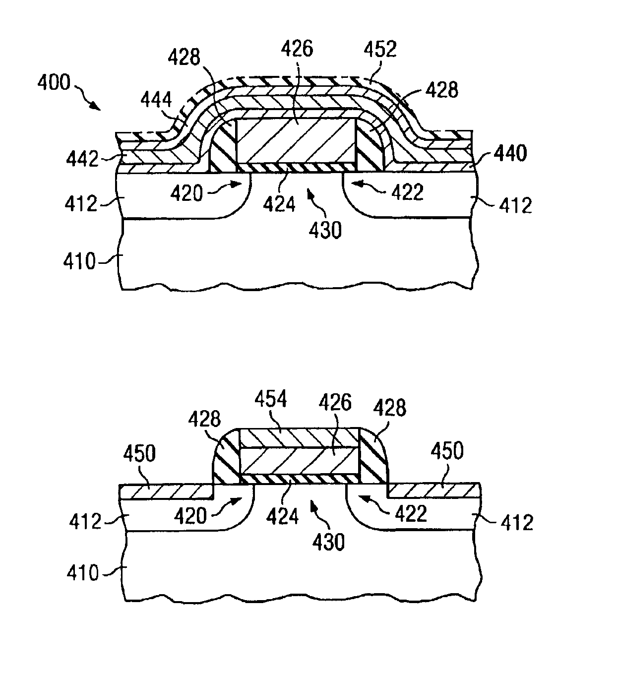
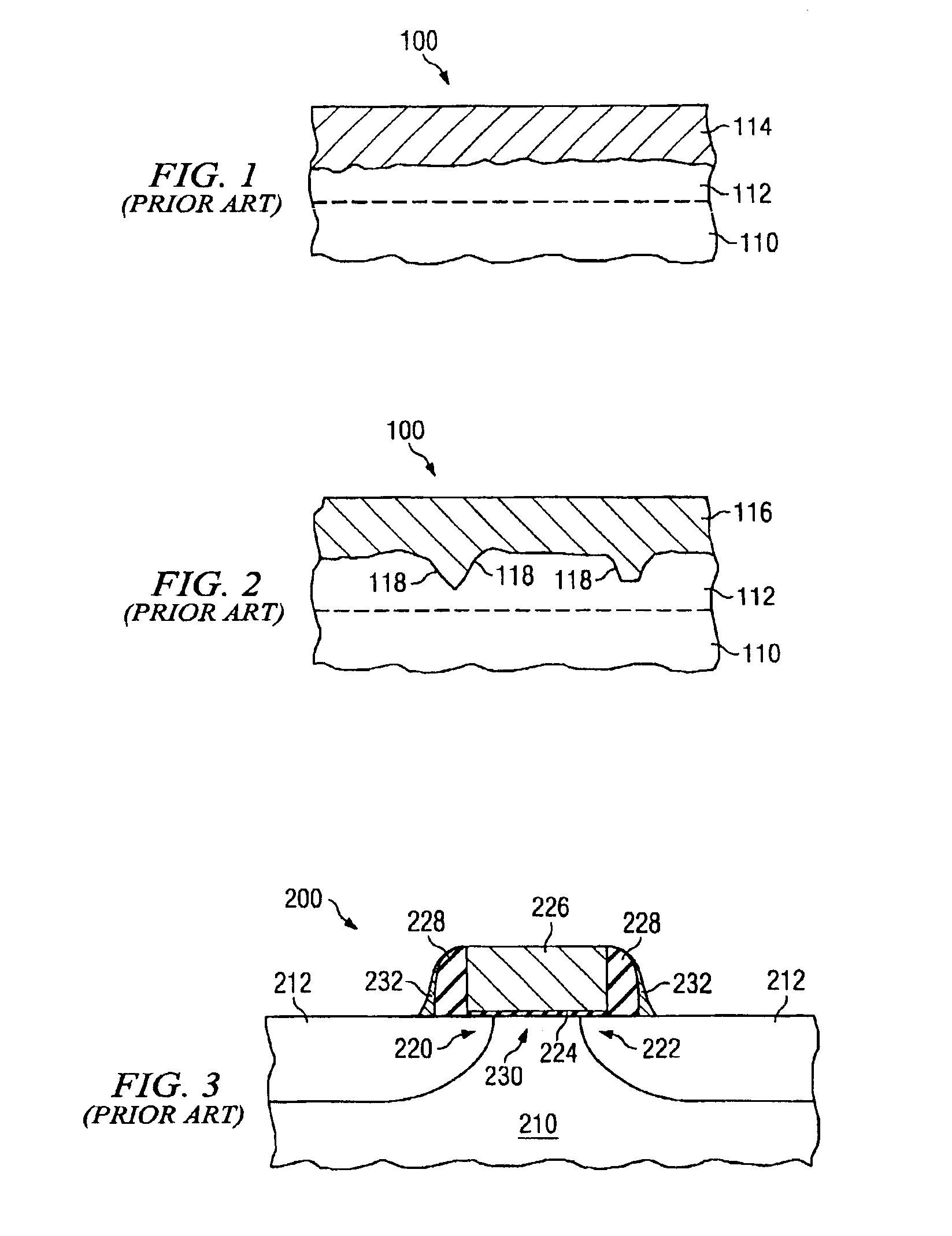
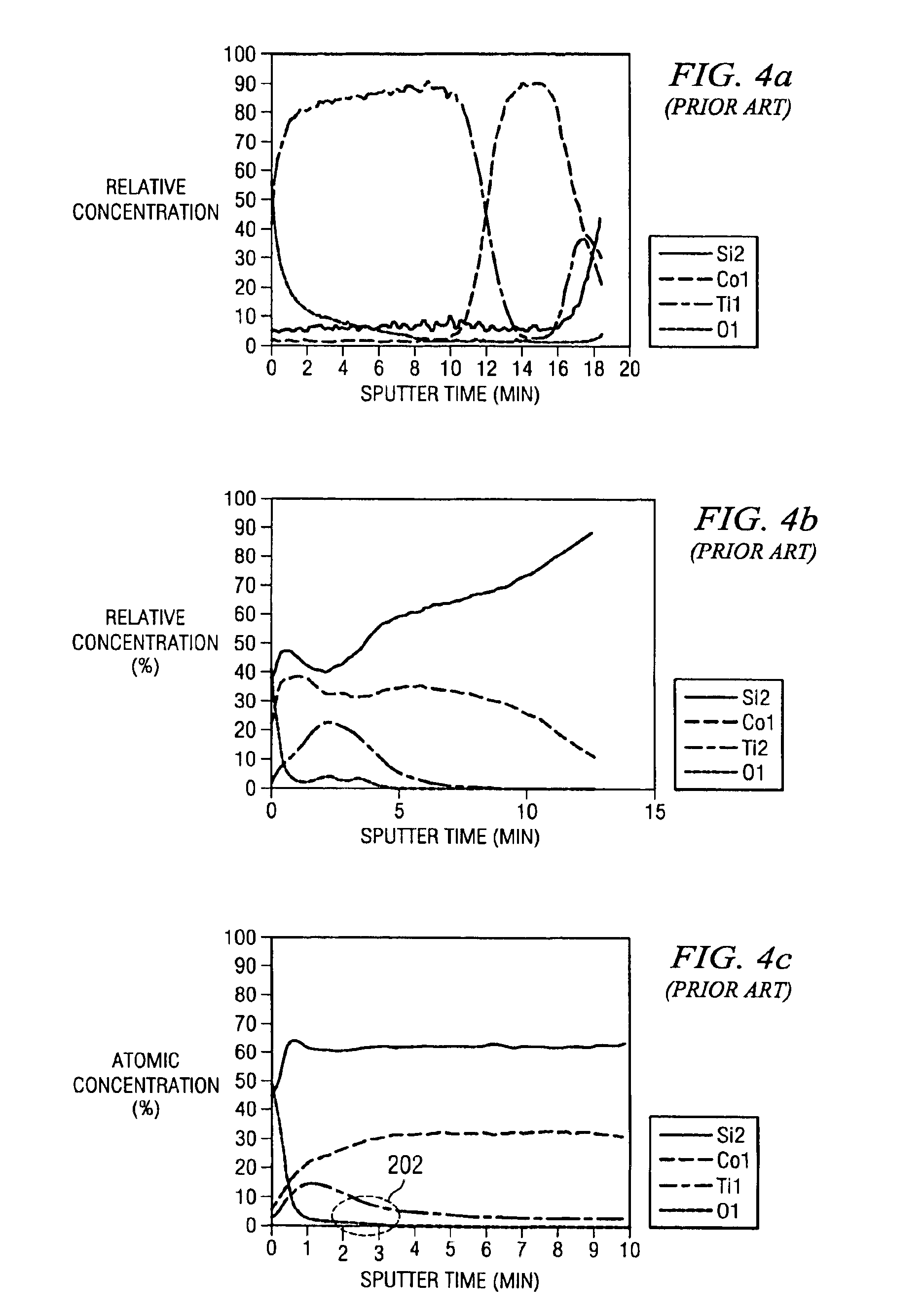
[0024]Problems with prior art cobalt silicide formation will be discussed, followed by a description of preferred embodiments of the present invention and some advantages thereof. The present invention will be described with respect to preferred embodiments in a specific context, namely a CMOS transistor. Embodiments of the invention may also be applied, however, to other semiconductor device applications where a silicide is desired to be formed.

[0025]Prior art methods of forming cobalt suicide will next be discussed. In FIG. 1, a semiconductor wafer or substrate 110 comprisi...


PUM

PropertyMeasurementUnit
temperatureaaaaaaaaaa
thicknessaaaaaaaaaa

Abstract

A method of forming a salicide on a semiconductor device includes depositing a first refractory metal layer over a silicon region of a substrate, depositing a near-noble metal layer over the first refractory metal layer, and depositing a second refractory metal layer over the near-noble metal layer. The semiconductor device is annealed in a first annealing process to form a silicide layer abutting the doped region of the semiconductor device. Un-reacted portions of the near-noble metal layer and the second refractory metal layer are removed. The device may be annealed in an optional second annealing process to convert the silicide layer to a low resistance phase silicide material. Junction leakage and bridging are minimized or eliminated by embodiments of the present invention, and a smoother silicided surface is achieved.

Description

TECHNICAL FIELD[0001]The present invention relates generally to semiconductor device fabrication, and more particularly to the formation of a salicide structure in semiconductor devices.BACKGROUND[0002]In semiconductor device manufacturing, suicides, which are alloys of silicon and metals, are often used. Silicides may be formed by the reaction of a refractory metal or a near-noble metal with silicon, and they are used in a variety of applications. For example, silicide may be used at the source / drain and / or gate area, or it may be used to construct a gate or local interconnect lines, as examples.[0003]A salicide is a Self-ALigned suicide; the term salicide refers to a silicide formed by a self-aligning method. A salicide is typically formed by depositing a metal layer over a silicon layer, and then annealing the semiconductor structure. Where the metal is in contact with the silicon, a silicide is formed. Un-reacted metal is then selectively etched away, leaving the silicide automa...

Claims


Application Information

Patent Timeline
Patent Type & Authority Patents(United States)
IPC IPC(8): H01L21/283H01L21/336H01L21/4763H01L29/78H01L21/70H01L21/02H01L21/44H01L21/321H01L21/3205H01L21/8238H01L29/66H01L27/085H01L27/092H01L21/28H01L21/285
CPCH01L21/28518H01L29/665H01L21/28052
Inventor FANG, SUNFEIWONG, KEITH KWONG HONAGNELLO, PAUL D.LAVOIE, CHRISTIANCLEVENGER, LAWRENCE A.DZIOBKOWSKI, CHESTER T.MURPHY, RICHARD J.DEHAVEN, PATRICK W.ROVEDO, NIVOHUANG, HSIANG-JEN
Owner IBM CORP
Why Eureka
Try Eureka