Semiconductor photocathode

a technology of semiconductor photocathode and photocathode, which is applied in the direction of discharge tube main electrode, image-conversion/image-amplification tube, and screen-mounted tubes, etc., can solve the problems of insufficient characteristics of semiconductor photocathode, shorten the transit time necessary for the passage of electrons, and suppress regions of overlapping electrons due to diffusion.

Inactive Publication Date: 2005-07-12
HAMAMATSU PHOTONICS KK
View PDF11 Cites 26 Cited by
  • Summary
  • Abstract
  • Description
  • Claims
  • Application Information

AI Technical Summary

Benefits of technology

[0011]In the case of a thick light-absorbing layer, such a phenomenon of a decrease in the time resolution occurs. However, when the thickness of a light-absorbing layer is limited as described above, a portion of low electron concentration in one electron group is cut out, and hence the above-described regions in which adjacent electron concentration distributions overlap each other decrease. Therefore, by shortening the transit time necessary for the passage of electrons, regions of overlapping electrons due to diffusion can also be suppressed. Furthermore, the strength of an electric field within a light-absorbing layer can be increased by thinning the light-absorbing layer. Therefore, the time resolution of infrared ra

Problems solved by technology

However, the characteristics of these semiconductor photocathode

Method used


Image

  • Semiconductor photocathode
  • Semiconductor photocathode
  • Semiconductor photocathode

Examples


first embodiment

(First Embodiment)

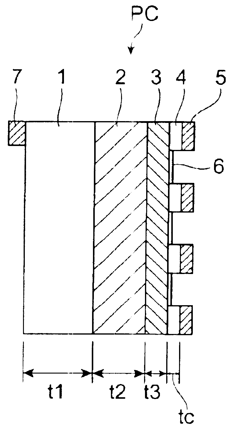
[0025]FIG. 1 is a longitudinal sectional view of a semiconductor photocathode PC related to a first embodiment. First, the construction of the semiconductor photocathode PC will be described.

[0026]The semiconductor photocathode PC of this embodiment, which is disposed in a vacuum opposing to an anode not shown in the figure, includes at least a light-absorbing layer 2, an electrode transfer layer 3, a contact layer 4 and an electrode layer 5 which are sequentially laminated on a semiconductor substrate 1. The contact layer 4 and electrode layer 5 are patterned in mesh (grid) form, and an active layer 6 is formed on an exposed surface of the electron transfer layer 3 at least within openings of this mesh.

[0027]Here, the explanation is given here by taking as an example a case where a grid pattern is used as the pattern of the contact layer 4 and electrode layer 5. However, various patterns can be applied as long as the electron transfer layer 3 is exposed in an almo...

second embodiment

(Second Embodiment)

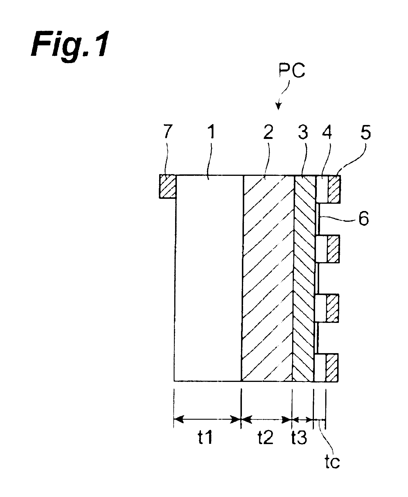
[0057]FIG. 2 is a longitudinal sectional view of a semiconductor photocathode PC related to a second embodiment. The semiconductor photocathode PC of the second embodiment differs from that of the first embodiment in that the formation of the contact layer 4 shown in FIG. 1 omitted, with the result that the electrode layer 5 and the electron transfer layer 3 are in direct Schottky contact with each other. Any materials can be used as the electrode material in this case as long as they come into Schottky contact with the electron transfer layer 3. However, a selection may be made in consideration of processes such as etching which are to be performed later. Other points of structure including the thickness of each layer and the like are the same as the photocathode of the first embodiment.

[0058]For the manufacturing method, the second embodiment differs from the first embodiment in that the formation of the contact layer 4 (Step (4)) is not performed after the form...

third embodiment

(Third Embodiment)

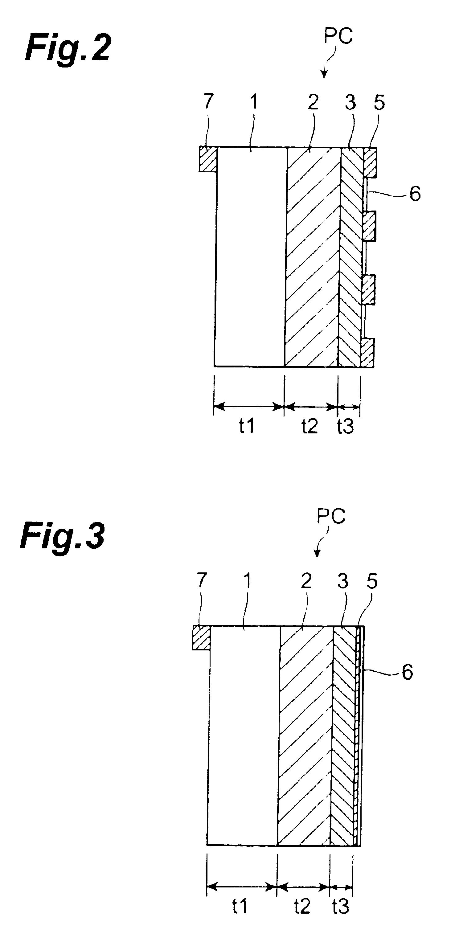
[0059]FIG. 3 is a longitudinal sectional view of a semiconductor photocathode PC related to a third embodiment. The semiconductor photocathode PC of the third embodiment differs from that of the second embodiment in that the electrode layer 5 shown in FIG. 2 is formed on the whole exposed surface of the electron transfer layer 3, that the thickness of the electrode layer 5 is small, and that the active layer 6 is formed on this thin electrode layer 5. Any materials can be used as the electrode material in this case as long as they come into Schottky contact with the electron transfer layer 3. Other points of structure including the thickness of each layer and the like are the same as those of the photocathode of the second embodiment.

[0060]The thickness of the electrode layer 5 has a great effect on the photoelectric conversion quantum efficiency of the photocathode. Specifically, when the thickness is smaller than a specific film thickness, the surface resistance ...


PUM


Abstract

In the case of a thick light-absorbing layer 2, a phenomenon of a decrease in the time resolution occurs. However, when the thickness of the light-absorbing layer 2 is limited, a portion of low electron concentration in one electron group is cut out, and hence overlap regions of adjacent electron concentration distributions decrease. Therefore, by shortening the transit time necessary for the passage of electrons, regions of overlapping electron distributions due to diffusion can also be suppressed. Furthermore, the strength of an electric field within a light-absorbing layer can be increased by thinning the light-absorbing layer. Therefore, the time resolution of infrared rays can be remarkably improved by a synergistic action of these effects. If it is assumed that the time resolution is 40 ps (picoseconds), for example, when the thickness of a light-absorbing layer is 1.3 μm which is nearly equal to the wavelength of infrared, then a possible time resolution is 7.5 ps when this thickness is 0.19 μm.

Description

TECHNICAL FIELD[0001]The present invention relates to a semiconductor photocathode.BACKGROUND ART[0002]Conventional semiconductor photocathodes are described in the U.S. Pat. No. 3,958,143, U.S. Pat. No. 5,047,821, U.S. Pat. No. 5,680,007 and U.S. Pat. No. 6,002,141. Such semiconductor photocathodes are provided with a light-absorbing layer formed from a compound semiconductor which absorbs infrared rays and emits electrons among carriers generated in response to the absorption of infrared rays through an electron transfer layer (an electron emission layer) into a vacuum.DISCLOSURE OF THE INVENTION[0003]However, the characteristics of these semiconductor photocathodes are not adequate as yet and further improvements are required. The present invention is made in view of such problems, and its object is to provide a semiconductor photocathode whose characteristics can be improved.[0004]A semiconductor photocathode according to the present invention, which includes a light-absorbing l...

Claims


Application Information

Patent Timeline
IPC IPC(8): H01J1/02H01J1/34H01J29/38H01J31/50H01J40/06
CPCH01J1/34H01J2201/3423H01L31/09
Inventor NIIGAKI, MINORUHIROHATA, TORUKAN, HIROFUMIMORI, KUNIYOSHI
Owner HAMAMATSU PHOTONICS KK
Why Eureka
Try Eureka