Fiber-based field emission display

Inactive Publication Date: 2005-07-12
MOORE CHAD BYRON
View PDF24 Cites 21 Cited by
  • Summary
  • Abstract
  • Description
  • Claims
  • Application Information

AI Technical Summary

Benefits of technology

[0007]Briefly stated, the invention pertains to the field of constructing a field emission display using an array of fibers and an orthogonal array of emitter electrodes. Each fiber in the fiber array contains an extraction electrode, spacer, a high voltage electrode and a phosphor layer. The ar

Problems solved by technology

One of the largest problems plaguing the FED industry is the ability to create support structures to maintain a millimeter-sized gap between the high-voltage plane and the emitter plane under hard vacuum.
The electronics needed to switch the high voltage fast enough to address every pixel in a reasonably sized display is presently impossible to construct.
Another pitfall

Method used


Image

  • Fiber-based field emission display
  • Fiber-based field emission display
  • Fiber-based field emission display

Examples


Embodiment Construction

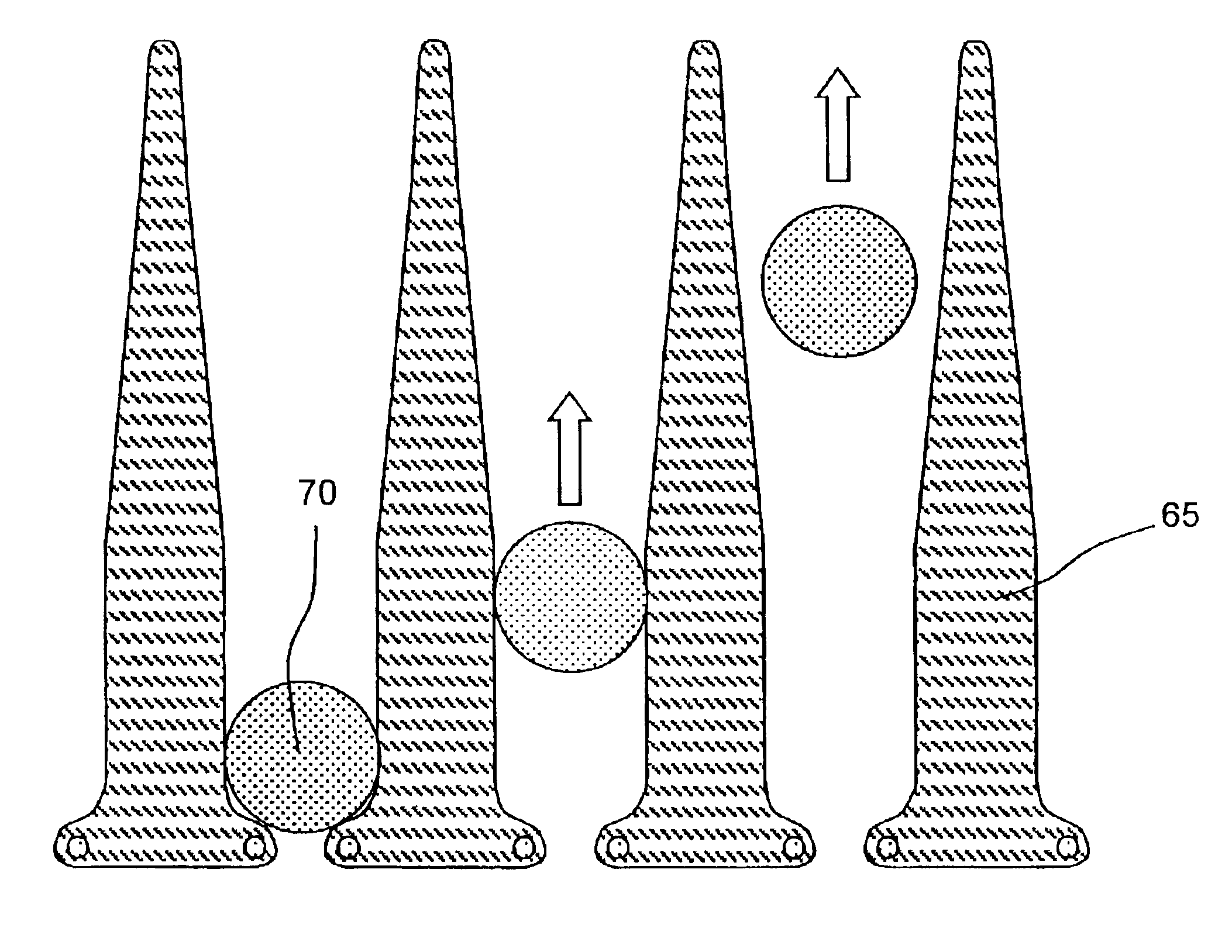
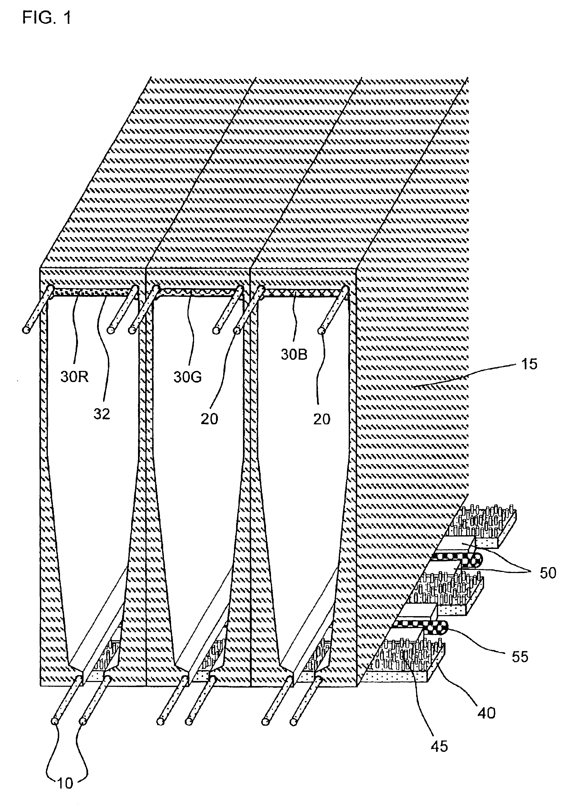
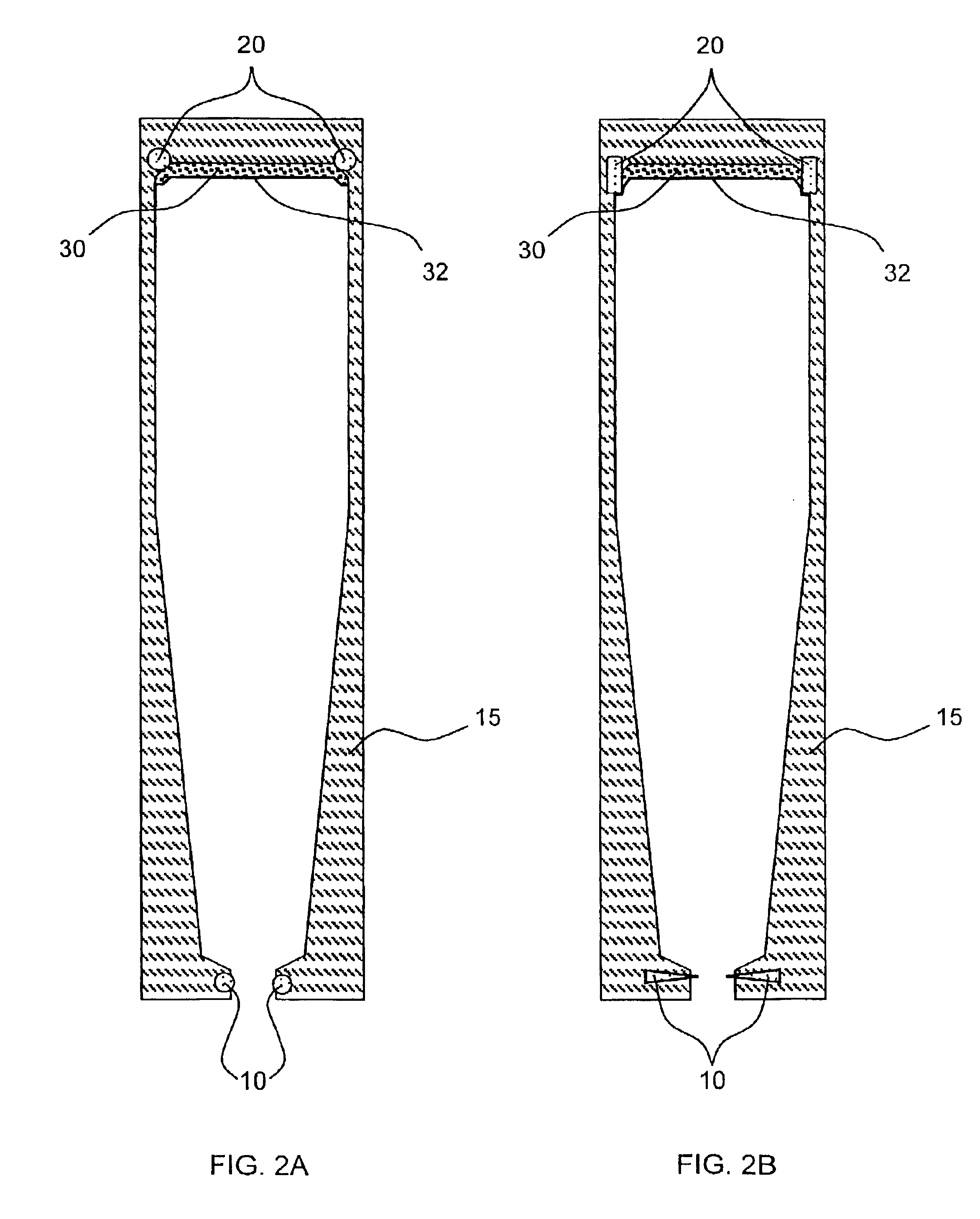
[0051]FIG. 1 shows a FED with one row of fibers 15 and an orthogonal row of emitter 45 electrodes 40. Each fiber 15 contains extraction electrodes 10, high voltage electrodes 20, phosphors 30R, 30G, 30B and a thin conductive coating 32 over the phosphor layers 30. The orthogonal array of emitter electrodes include carbon nanotube emitters 45 attached to a conductive electrode 40. The conductive electrodes 40 are separated by non-conductive spacers 50. Between the non-conductive spacers 50 are getter wires 55. In order to operate the FED, shown in FIG. 1, it needs to be enclosed in a vacuum vessel not shown. A vacuum vessel can be formed by sandwiching the structure, shown in FIG. 1, between to glass plates and frit sealing the glass plates around the perimeter. The wire electrodes can be brought out through the frit seal region and connected to the drive electronics.

[0052]Operation of the FED, shown in FIG. 1, is achieved by applying a voltage on the extraction electrodes 10 with re...


PUM

PropertyMeasurementUnit
Shapeaaaaaaaaaa

Abstract

The invention relates to a field emission display constructed using an array of fibers and an orthogonal array of emitter electrodes. Each fiber in the fiber array contains an extraction electrode, spacer, a high voltage electrode and a phosphor layer. The array of emitter electrodes consists of carbon nanotube emitters attached to conductive electrodes. The emitter electrodes are separated using non-conductive fibers. A getter material in the form of a wire is placed within the array of emitter electrodes to maintain a high vacuum within the display.

Description

REFERENCE TO RELATED APPLICATIONS[0001]This is a divisional patent application of application Ser. No. 09 / 797,383, filed Mar. 1, 2001 now U.S. Pat. No. 6,507,146, entitled “FIBER-BASED FIELD EMISSION DISPLAY”. The aforementioned application is hereby incorporated herein by reference.[0002]Application Ser. No. 09 / 797,383 claims an invention which was disclosed in Provisional Application No. 60 / 186,024, filed Mar. 1, 2000, now abandoned, entitled “FIBER-BASED FIELD EMISSION DISPLAY”. The benefit under 35 USC §119(e) of the United States provisional application is hereby claimed, and the aforementioned application is hereby incorporated herein by reference.FIELD OF THE INVENTION[0003]The invention pertains to the field of creating a field emission display using an array of fibers and an orthogonal array of emitter electrodes. The invention further relates to using carbon nanotubes as the electron emitters. The invention further relates to using a metal-insulator-metal cathode for the e...

Claims


Application Information

Patent Timeline
IPC IPC(8): C03B37/16C03B37/03C03B37/026C03B37/025C03B37/02C03B37/10C03B37/14C03C27/06G02F1/133G02F1/13G09G3/36H01J29/94G09G3/28H01J29/00H01J31/12H01J29/02H01J9/24H01J17/16H01J17/02H01J9/18H01J29/86
CPCB82Y10/00C03B37/025C03B37/026C03B37/03C03B37/14C03B37/16C03C27/06G02F1/13334H01J9/185H01J9/242H01J29/028H01J29/864H01J29/94H01J31/123H01J2201/30469H01J2329/863
Inventor MOORE, CHAD BYRON
Owner MOORE CHAD BYRON
Why Eureka
Try Eureka