Semiconductor-based encapsulated infrared sensor and electronic device

a technology of infrared sensor and semiconductor, applied in the field of semiconductor-based encapsulated infrared sensor and electronic device, can solve the problems of high percent of defective devices, deterioration of vacuum, and broken wafers, and achieve the effect of increasing the function of holding the atmosphere and strong joining

Inactive Publication Date: 2005-11-15
PANASONIC HLDG CORP
View PDF19 Cites 31 Cited by
  • Summary
  • Abstract
  • Description
  • Claims
  • Application Information

AI Technical Summary

Benefits of technology

[0010]A second object of the present invention is to improve the function of electronic devices such as infrared sensors, by taking measures for providing a higher degree of vacuum in the inside space in which an cell array is placed.
[0041]In the above described step (a), a first ring-shaped film enclosing a plurality of cell regions is formed on the above described main body substrate and a second ring-shaped film having approximately the same pattern as said first ring-shaped film is formed on the above described cap substrate, and thereby it is possible to realize strong joining by selecting materials forming first and second ring-shaped portions.

Problems solved by technology

First, when a large number of elements such as infrared detectors are arranged in an array-like configuration, it is difficult to make the whole joining portion at the periphery of the cell array completely flat, and thus an excessively high push pressure is inevitably required for thermal pressure bonding, thereby causing the possibility of broken wafers during joining, deteriorated vacuum caused by residual stress and device malfunctions.
Second, if a joining failure is caused at part of the joining portion for maintaining elements such as a large number of infrared detectors under vacuum, the vacuum is broken over the whole cell array, and thus the whole device becomes bad, thus resulting in a high percent of defective devices.
Third, when solder is used for the joining, the degree of vacuum in the inside space having the cell array placed therein can not be higher than a certain level because of outgassing of organic materials included in the solder paste. Therefore, there has been the possibility that an increase in the sensitivity of infrared sensors can not be expected, for example.

Method used


Image

  • Semiconductor-based encapsulated infrared sensor and electronic device
  • Semiconductor-based encapsulated infrared sensor and electronic device
  • Semiconductor-based encapsulated infrared sensor and electronic device

Examples


embodiment 1

[0100]Next, description will be made for an embodiment 1 applying the electronic device according to the invention to a discrete type of infrared sensor.

[0101]FIGS. 4A and 4B are a cross-sectional view and an electrical circuit for illustrating an infrared sensor according to Embodiment 1 of the invention, respectively.

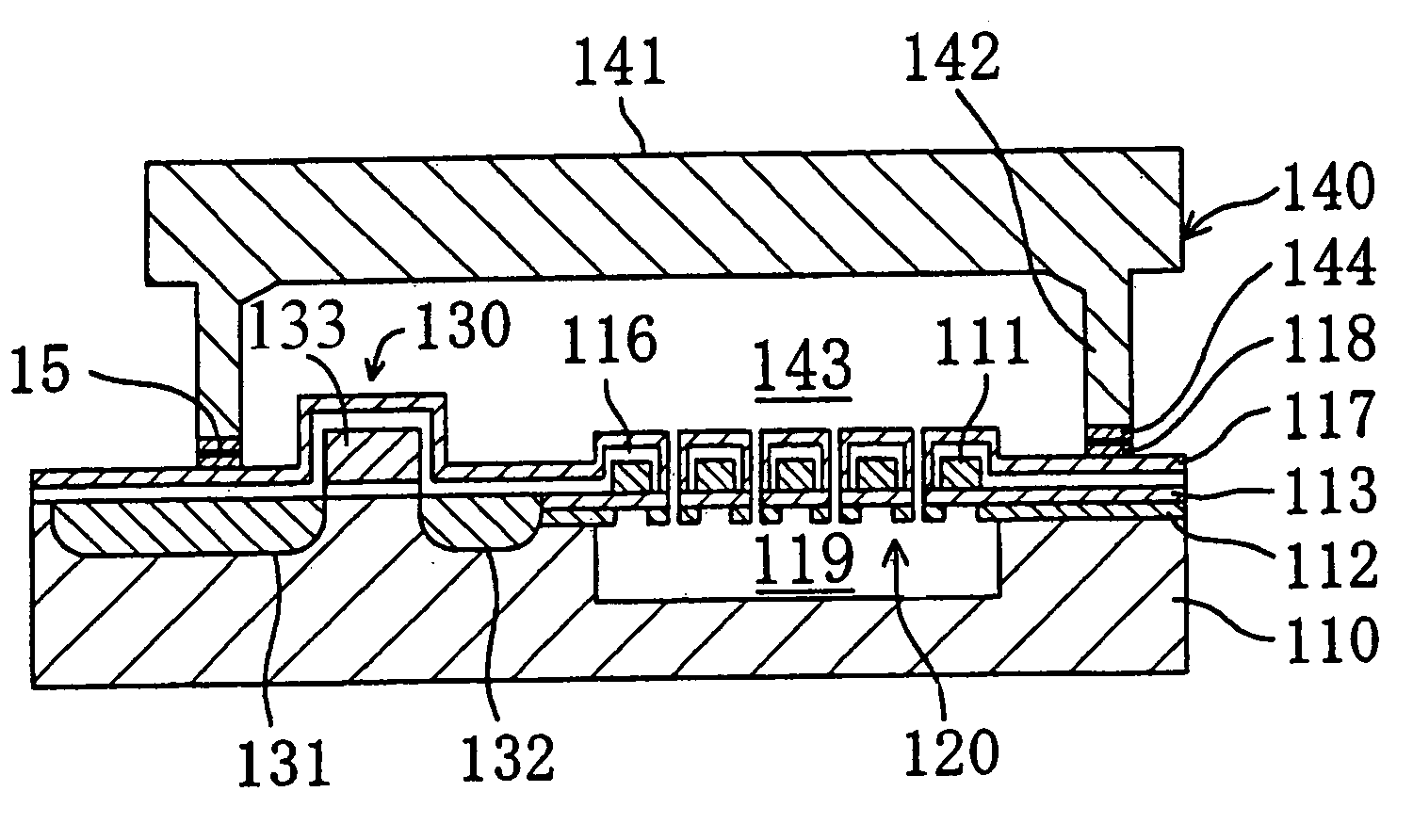
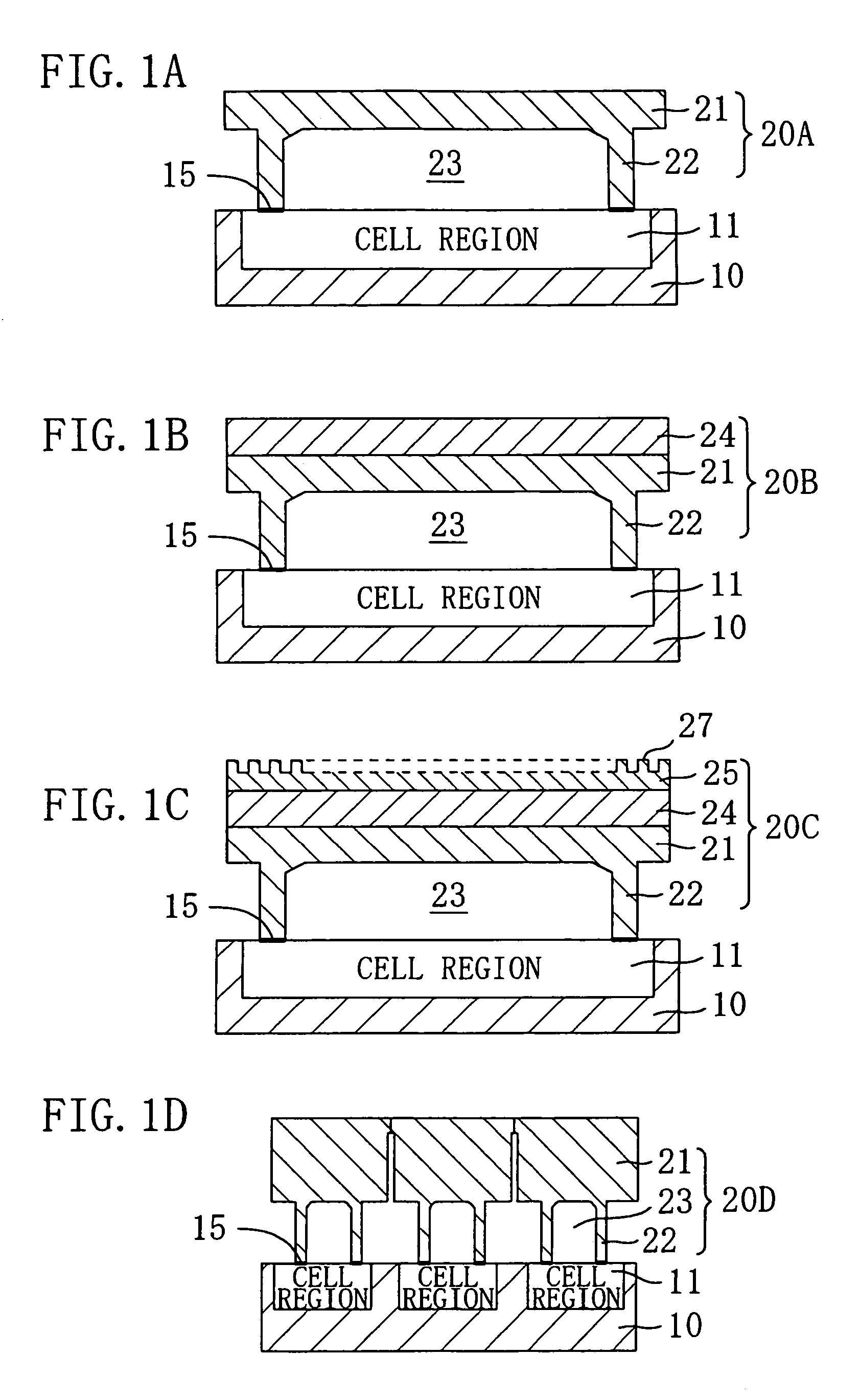
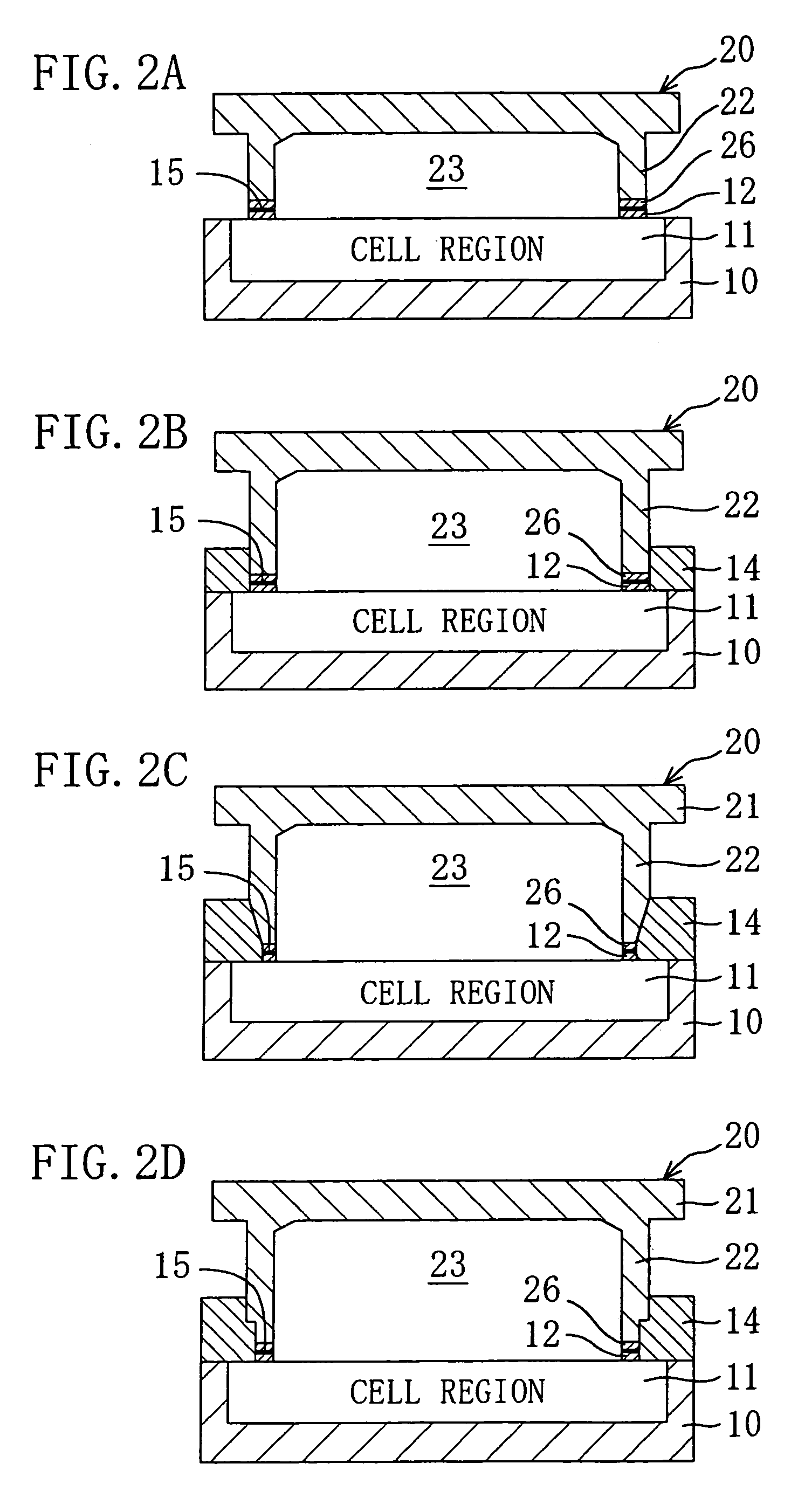
[0102]As shown in FIG. 4A, the infrared sensor of the present embodiment comprises a Si substrate 110 having a thickness of 300 μm, a resistance element (bolometer) 120 provided on the Si substrate 110, a switching transistor 130 provided on the Si substrate 110 for turning on and off a current to the resistance element 120, and a cap body 140 for holding the area having the resistance element 120 placed thereon in an atmosphere of reduced pressure. The total size of this infrared sensor is about several mm. Above the Si substrate 110, there are provided the resistance body 111 patterned into a fanfold (Z-fold)-shape, a silicon nitride film 112 and a silicon oxide fil...

embodiment 2

[0150]FIG. 9 is an electrical circuit for illustrating the configuration of an infrared area sensor according to Embodiment 2 of the invention. The concrete structure of the infrared area sensor according to the present embodiment is shown in FIG. 13.

[0151]As shown in the same drawing, a main body substrate is provided with a cell array in which a large number of cells A1–E5 each having a bolometer 201 and a switching transistor 202 are disposed in matrix-like arrangement. Although the size of one cell is, for example, about 40 μm–50 μm, the size is adequate to be larger than 20 μm corresponding to about two times the wavelength of infrared radiation to be detected. The gate electrodes of the switching transistors 202 in each cell are connected to selection lines SEL-1-SEL-5 extending from a vertical scanning circuit 209 (V-SCAN). One end of the bolometer 201 in each cell is connected to a power supply line 205, the sources of the switching transistors 202 are connected to data line...

embodiment 3

[0165]FIG. 12 is a cross-sectional view for showing an example of a micro vacuum transistor having a vacuum dome structure according to Embodiment 3 of the invention. The micro vacuum transistor according to the present embodiment comprises a sapphire substrate 201, an n-GaN layer 202 provided on the sapphire substrate 201 and functioning as an electron supplying layer, an AlxGa1−xN layer 203 provided on n-GaN layer 202 and configured as a composition gradient layer having composition approximately continuously changed and functioning as a electron drift layer, an AlN layer 204 provided on the AlxGa1−xN layer 203 and functioning as a surface layer, a lower electrode 205 provided on the n-GaN layer 202, a surface electrode 206 provided on the ALN layer 204 and forming a Schottky contact with the AlN layer 204, and a first insulating film 207 provided on the AlN layer 204 and having an opening portion. Further, a thin film portion 206a of the surface electrode 206 is formed on the reg...


PUM


Abstract

An Al film is formed on a cap wafer and the Al film is patterned into a ring-shaped film. Dry etching is performed by using the ring-shaped film as a mask to form a drum portion enclosing a recess portion to provide a vacuum dome. After forming a depth of cut into the substrate portion of the cap wafer, the cap wafer is placed on a main body wafer having an infrared area sensor formed thereon. Then, the ring-shaped film of the cap wafer and the ring-shaped film of the main body wafer are joined to each other by pressure bonding to form a ring-shaped joining portion.

Description

CROSS-REFERENCE TO RELATED APPLICATIONS[0001]This application is a divisional of U.S. patent application Ser. No. 10 / 163,691 filed on Jun. 6, 2002 now U.S. Pat. No. 6,890,834. The disclosure(s) of the above application(s) is (are) incorporated herein by reference. This application claims the benefit of Japanese Patent Application No. 2001-176184 filed Jun. 11, 2001.BACKGROUND OF THE INVENTION[0002]The present invention relates to electronic devices, such as sensors and transistors, configured to be sealed in an atmosphere of reduced pressure or an atmosphere of inert gas.[0003]Conventionally, electronic devices exhibiting high performance in an atmosphere of vacuum (or atmosphere of reduced pressure), such as infrared sensors and vacuum transistors, are typically sealed in a case of hermetic seal and ceramic or the like for use thereof. Such vacuum-packaged electronic devices include a so-called discrete type of device having a single sensor disposed therein and an integration type ...

Claims


Application Information

Patent Timeline
Patent Type & Authority Patents(United States)
IPC IPC(8): B81B7/00H01L23/02H01L23/10H01L25/00G01J5/10H01L27/146H01L31/0203
CPCB81B7/0077H01L23/10H01L27/14618H01L27/14649H01L27/14687H01L31/0203G01J5/10H01L27/14609H01L2924/01079H01L2924/16235H01L2924/0002H01L2924/00H01L25/00
Inventor KOMOBUCHI, HIROYOSHIKUBO, MINORUHASHIMOTO, MASAHIKOOKAJIMA, MICHIOYAMAMOTO, SHINICHI
Owner PANASONIC HLDG CORP
Why Eureka
Try Eureka