Reactive deposition for the formation of chip capacitors

Inactive Publication Date: 2005-07-12
NANOGRAM
View PDF40 Cites 13 Cited by
  • Summary
  • Abstract
  • Description
  • Claims
  • Application Information

AI Technical Summary

Benefits of technology

[0009]In a further aspect, the invention pertains to a ceramic chip capacitor having at least two layers of electrical conductor and at least one layer of dielectric between the electrical conducting layers. The dielectric layers include a collection of particles having a

Problems solved by technology

However, sintering of the dielectric material in a reducing atmosphere can result in the reduction of the die

Method used


Image

  • Reactive deposition for the formation of chip capacitors
  • Reactive deposition for the formation of chip capacitors
  • Reactive deposition for the formation of chip capacitors

Examples


Embodiment Construction

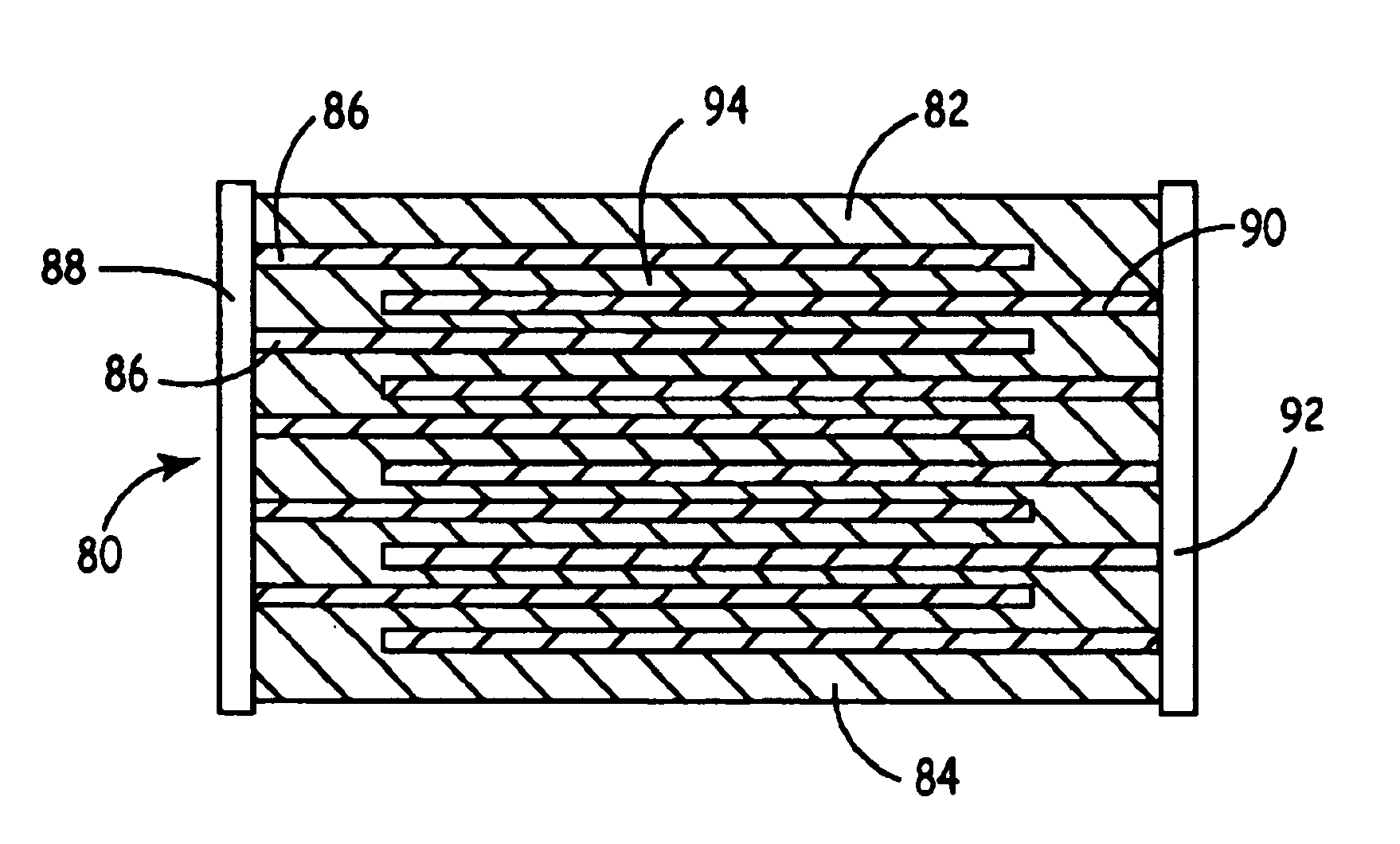
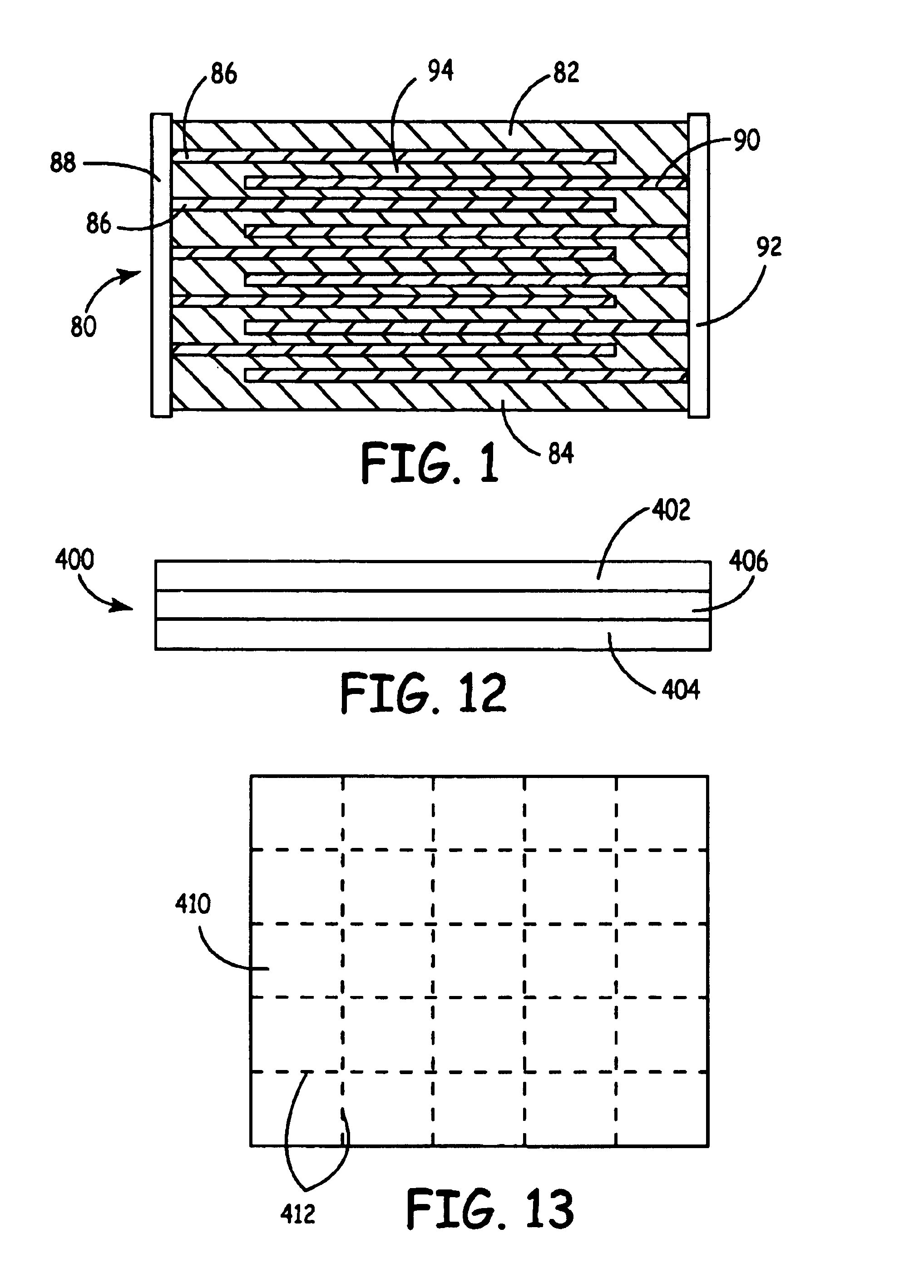
[0029]Dielectric materials and / or electrical conducting materials for chip capacitors can be deposited in layers as the materials are produced in a flowing reactant system. By depositing the materials with a flow reactor, the process for the formation of chip capacitors can be streamlined since the particles are deposited without collecting the particles in a separate collector. The light reactive deposition process is extremely flexible with respect to selection of the composition of the materials in the dielectric layer. In addition, extremely small particles can be deposited for the formation of the dielectric materials. Similarly, elemental metal particles can be deposited for the formation of the electrodes. In light reactive deposition, each layer can be formed by movement of the substrate past a particle flow from a light reaction zone. Thus, all the layers of a multi-layer structure can be formed by repeated passes through the coating stream. The composition of the reactant ...


PUM

PropertyMeasurementUnit
Percent by massaaaaaaaaaa
Diameteraaaaaaaaaa
Diameteraaaaaaaaaa

Abstract

Methods for the production of ceramic chip capacitors include the deposition of at least two layers of electrical conductor and at least one layer of a dielectric between electrical conducting layers. The compositions in the dielectric layer are deposited from a flow in which flowing reactants react to form particles in a reaction driven by light at a light reaction zone. In some embodiments, a plurality of dielectric layers is deposited. Suitable dielectric materials include barium titanate. A collection of barium titanate particles can be formed in the coating process having an average diameter less than about 90 nanometers. Thus, ceramic chip capacitors can be formed with barium titanate particles having an average diameter less than about 90 nanometers.

Description

CROSSREFERENCE TO RELATED APPLICATIONS[0001]This application claims priority to copending U.S. Provisional Patent Application No. 60 / 312,234, filed Aug. 14, 2001, to Bryan, entitled “Reative Deposition For The Formation Of Chip Capacitors,” incorporated herein by reference.FIELD OF THE INVENTION[0002]The invention relates to chip capacitors with dielectric compositions separating electrodes in a multi-layer construction. The invention further relates to reactive deposition of dielectric materials with light driving the reaction for the formation of a multi-layer capacitor.BACKGROUND OF THE INVENTION[0003]Small multi-layer chip capacitors are used in various electronic devices due to their high capacity, high reliability and compact size. Along with demands for continuing reductions in size and improved reliability, there has been increasing demands for price reductions and increased capacity. Conventional approaches for the production of ceramic chip capacitors involve the applicati...

Claims


Application Information

Patent Timeline
IPC IPC(8): H01G4/08H01G4/12H01G13/00
CPCH01G4/08H01G13/00H01G4/12Y10T29/43
Inventor BRYAN, MICHAEL A.
Owner NANOGRAM
Why Eureka
Try Eureka