Multichip module

a multi-chip module and chip technology, applied in the field of multi-chip modules, can solve the problems of high thermal stress, high reliability concerns, disadvantageous for high-density integrated circuit development, etc., and achieve the effects of reducing thermal stress difference, preventing chip cracking or even breaking wires, and reducing thermal expansion coefficient of adhesives

Inactive Publication Date: 2005-07-19
SILICONWARE PRECISION IND CO LTD
View PDF5 Cites 51 Cited by
  • Summary
  • Abstract
  • Description
  • Claims
  • Application Information

AI Technical Summary

Benefits of technology

[0010]A primary objective of the present invention is to provide a multichip module and a manufacturing method thereof, which simplifies and reduces the time for the manufacturing procedures as well as reducing the overall manufacturing cost. Another objective of the present invention is to provide a multichip module and a manufacturing method thereof, in which the differences in coefficient of thermal expansion between the topmost, bottommost chip and that of the adhesive layer interposed in between are greatly reduced, so as to prevent delamination at the chip bonding surface, chip cracking or broken wires from accordance, and ultimately enhancing the yield for the packaged product. Further, another objective of the present invention is to provide a multichip module and a manufacturing method thereof in which the heat dissipating efficiency of the topmost and bottommost chip is enhanced, thereby solving the heat retaining problem. Yet another objective of the present invention is to provide a multichip module and a manufacturing method thereof, in which the fluidity of the adhesive is reduced, allowing a preferred planarity of the topmost chip adhered onto the adhesive layer to be maintained. Yet another objective of the present invention is to provide a multichip module and a manufacturing method thereof, in which the chips have not size limitation. Further another objective of the present invention is to provide a multichip module and a manufacturing method thereof, in which the thickness of the adhesive layer interposed can be reduced, thereby reducing the overall height of the packaged product. Further, another objective of the present invention is to provide a multichip module and a manufacturing method thereof, in which a method is proposed such that the topmost chip cannot make contact with the bottommost chip, thereby eliminating the occurrence of broken wires and shortage.
[0014]Yet, in another embodiment of the present invention, reverse bonding technique is utilized to substantially reduce the loop height of the first bonding wires, allowing fillers with smaller diameters to be used, so as to reduce the thickness of the adhesive, and thereby achieving the objective of reducing the overall height of a semiconductor package.
[0016]The fillers can be made by dielectric polyimide, copper, aluminum, other alloys or other stiff and conductive materials. Addition of fillers into adhesive could change the characteristics of the adhesive, which in turn reducing the coefficient of thermal expansion of the adhesive thereby reducing thermal stress difference between the adhesive, chip and bonding wires, preventing the wire bonding surface from delamination, chip cracking or even broken wires. Moreover, addition of solid fillers into adhesive can effectively reduce the fluidity of the adhesive, which in tern preventing deviation of the second chip after mounting on the adhesive layer, and thereby a preferred planarity can be achieved. Fillers made by metal materials could also enhance the heat dissipation of the chip, thereby solving heat-retaining problem for the stacked multichip structure.

Problems solved by technology

This increased chip carrier surface will generate a higher thermal stress, and therefore resulting in a warpage of the chip carrier and subsequently an occurrence of delamination at the interface between the chip and the chip carrier, making this method facing much more reliability concerns.
In such a case, the top-most chip would have the smallest size, that is, the surface for disposing electronic circuits and electronic elements is reduced, which is disadvantageous for developing high-density integrated circuits.
However, when using insulated tapes made by adhesive materials such as polyimide for adhering the second chip 64, because of the high fluidity the planarity of the second chip 64 is difficult to achieve.
Moreover, because of the Coefficient of Thermal Expansion (CTE) differences between the adhesive materials and the chip is great, during temperature cycles of the latter procedures the chip bonding surface may be easily suffered from warpage, delamination or even chip cracking.
The foregoing method although can successfully overcome the problem of differences in CTE between the chip and the insulator apparatus, this method is costly and the manufacturing procedures is complex and prolonged, making the final yield difficult to enhanced.
Moreover, as adhesives of high fluidity is required to be applied over the active surface of the first chip or the surface of the insulator apparatus prior to bonding between the insulator apparatus and the topmost chip (i.e. the second chip), it is common that the adhesives would lead to the deviation of the insulator or the topmost chip or even damage the first chip pads.
However, one drawback is that for to the above-mentioned reverse bonding technique, the formation of a plurality of studs on the first chip for wire bonding is required prior to reverse bonding, making the procedures longer and costly.
In addition, as the Coefficient of Thermal Expansion (CTE) between the adhesive and the gold wires is great, the gold wires embedded in the adhesive may be easily broken due to different thermal stress under thermal cycles at latter procedures and as a result, the electronic performances of gold wires may be seriously impaired.
Besides, during bonding of the second chip, a highly accurate control equipment must be additionally incorporated to accurately control the bond force of the second chip against the adhesive layer, which further increases the overall manufacturing cost.

Method used


Image

  • Multichip module
  • Multichip module
  • Multichip module

Examples


first preferred embodiment

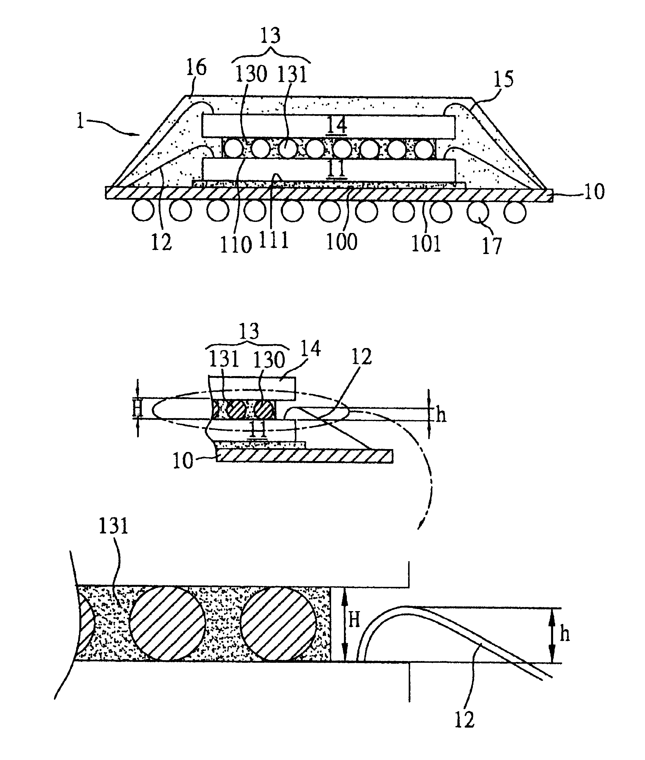
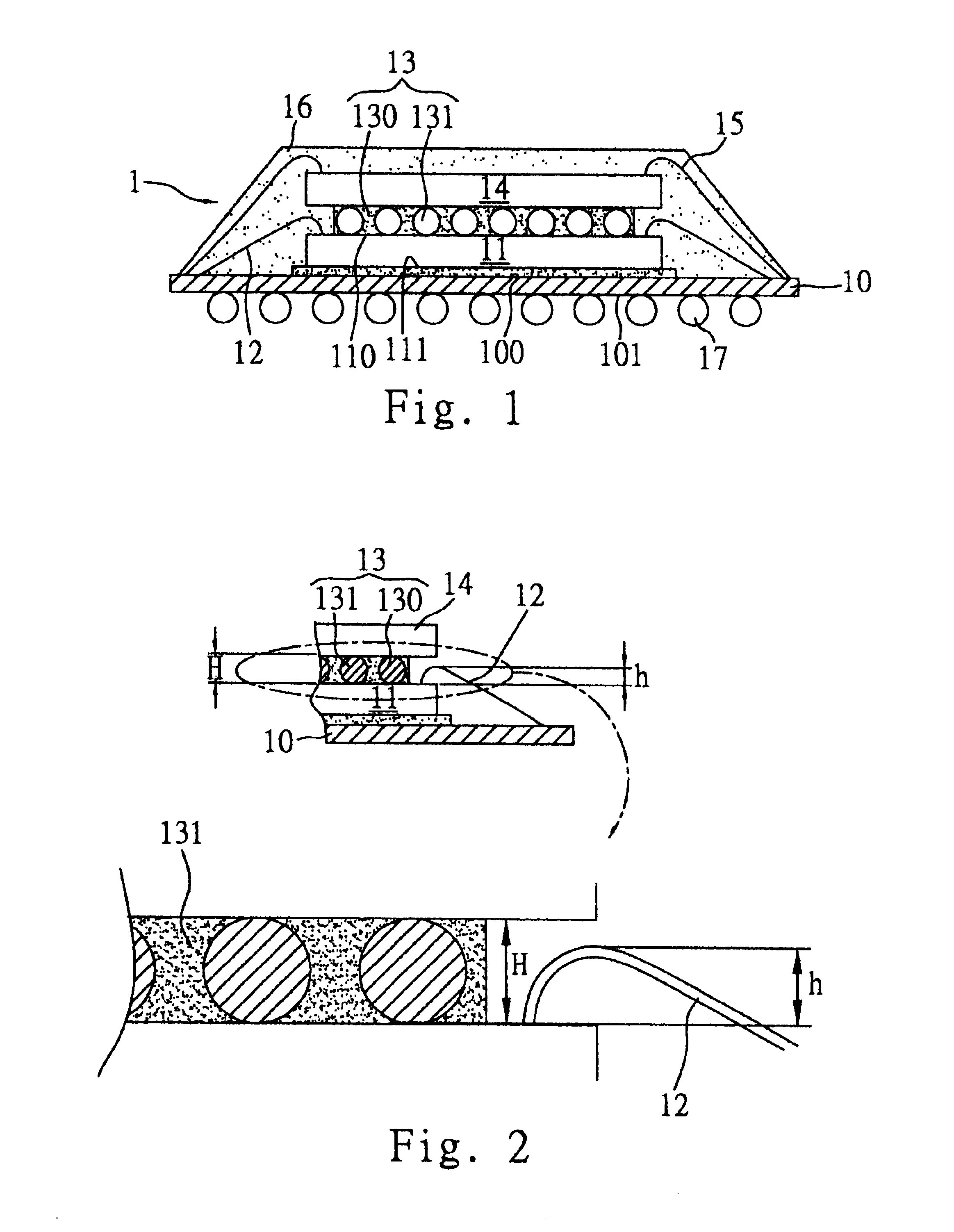
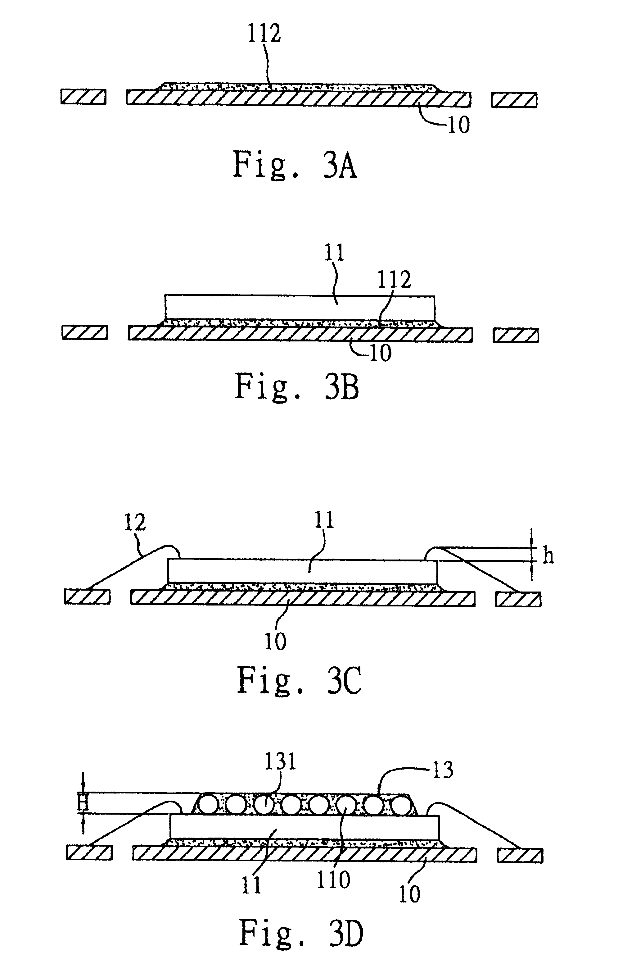
[0030]Illustrated in FIG. 1 is a cross-sectional schematic view of a multichip module according to a first embodiment of the present invention. As shown in the diagram, the semiconductor package 1 comprises: a substrate 10; a first chip 11 adhered onto the substrate 10; a plurality of gold wires 12 for providing electrical connection between the substrate 10 and the first chip 11; an adhesive layer 13 applied over the first chip 11; a second chip 14 adhered to the adhesive layer 13; a plurality of second gold wires 15 for providing electrical connection between the second chip 14 and the substrate; and an encapsulant 16 for encapsulating the first chip 11, the first gold wires 12, the second chips 14 and the second gold wires 15.

[0031]The substrate 10 is commonly used as a duel-chip stack substrate or multi-chip stack substrate, which is made by forming a core layer made of materials such as resin, ceramic, or fiberglass and forming conductive trace pattern on the upper and lower su...

second preferred embodiment

[0042]Illustrated in FIG. 4 is a cross-sectional schematic view of a multichip module according to a second embodiment of the present invention. As shown in the drawing, a multichip semiconductor package 2 of the second preferred embodiment is structurally similar to that of the foregoing first preferred embodiment, with the only difference in that, after wire bonding of the second bonding wires 25, an adhesive 23 is further applied over the active surface 240 of the second chip 24 whereon bonding pads are not disposed. This adhesive layer 23 is used for adhering at least one third chip 28 above the second chip to form a multichip semiconductor module 2 with three chips stacked perpendicularly on a substrate 20. The adhesive 23 applied on the second chip 24 also contains a plurality of fillers 231 of predetermined diameter as such, the diameter of the fillers 231 must be larger than the loop height (h′) of the second bonding wires 25. Thus, like the foregoing second chip 24, the siz...

third preferred embodiment

[0043]Illustrated in FIG. 5 is a cross-sectional schematic view of a multichip module according to a third embodiment of the present invention. As shown in the drawing, a multichip semiconductor package 3 of the third preferred embodiment is structurally similar to that of the foregoing first preferred embodiment, with the only difference in that, the wire bonding manner for the first bonding wires 32 is by utilizing reverse bonding technique; that is forming studs on each of the bonding pads disposed on the active surface 310 of the first chip 31 and bonding one end of the first gold wires 32 to the bonding pads (not shown) on the substrate 30 and then pulling each gold wires 32 upwardly allowing the other end thereof to be stitch bonded to the studs 320. With the use of reverse bonding technique, the wire loops can be modified, allowing the loop height above the first chip 31 to become very small (approx. under 2 mils). Thus, fillers 331 of smaller diameter can be used, so as to r...


PUM


Abstract

A multi-chip module is proposed, which is designed to pack two or more semi-conductor chips in a stacked manner over a chip carrier in a single package. The multi-chip module is characterized by the use of adhesive with fillers to allow the topmost chip (i.e. the second chip) superimposed to the bottommost chip (i.e. the first chip) after the first chip electrically connected to the chip carrier. The thickness of the adhesive layer depends on the diameter of the fillers higher than loop height of the bonding wires that is positioned above the active surface of the first chip to prevent the bonding wires connected to the first chip to come in contact with the overlaid chip.

Description

FIELD OF THE INVENTION[0001]The present invention relates to multichip modules (MCM) and a manufacturing method thereof, and more particularly to a multichip module having more than two chips disposed on a chip carrier in a stacked manner and a manufacturing method thereof.BACKGROUND OF THE INVENTION[0002]With increasing demands for higher electronic performances and miniaturization, multichip module arrangement has become a trend. Multichip module is an apparatus having at least 2 chips adhered onto a single chip carrier such as a substrate or a leadframe. The chip-to-chip carrier bonding manner can be generally categorized into two: One method is by spacing chips next to each other on a chip carrier. This bonding method essentially would not increase the overall height of the semiconductor package, but the chip carrier must contain a large area of die attachment area as to accommodate the required chip numbers. This increased chip carrier surface will generate a higher thermal str...

Claims


Application Information

Patent Timeline
Patent Type & Authority Patents(United States)
IPC IPC(8): H01L25/065
CPCH01L24/29H01L24/33H01L24/83H01L25/0657H01L2225/0651H01L2225/06575H01L2225/06582H01L2924/01013H01L2924/01029H01L2924/01047H01L2924/01079H01L2924/01082H01L2924/14H01L2924/15311H01L2924/19041H01L2224/48091H01L2924/00014H01L2224/32145H01L2224/32225H01L2224/32245H01L2224/4809H01L2224/48227H01L2224/48247H01L2224/83192H01L2224/838H01L2224/92247H01L2224/29H01L2224/2919H01L2924/01006H01L2924/01033H01L2924/014H01L2924/0665H01L2224/29101H01L2924/0132H01L2924/01014H01L2924/01007H01L2924/01074H01L2224/45144H01L2924/00H01L2224/73265H01L2924/3512H01L2924/00013H01L2224/29099H01L2224/29199H01L2224/83138H01L2924/00012H01L2224/29324H01L2224/2929H01L2224/293H01L2224/29347H01L2224/29386H01L2924/05032H01L2224/29299H01L2924/351H01L2924/181H01L24/73H01L23/02
Inventor LIU, CHUNG-LUNCHANG, CHIN-HUANG
Owner SILICONWARE PRECISION IND CO LTD
Why Eureka
Try Eureka