Molecular-junction-nanowire-crossbar-based inverter, latch, and flip-flop circuits, and more complex circuits composed, in part, from molecular-junction-nanowire-crossbar-based inverter, latch, and flip-flop circuits

a crossbar and circuit technology, applied in the field of electrical circuits, can solve the problems of extremely high densities and very little power consumption of nanowire crossbar implementations of circuits, and achieve the effect of high densities and little power

Inactive Publication Date: 2005-07-19
HEWLETT PACKARD DEV CO LP
View PDF9 Cites 269 Cited by
  • Summary
  • Abstract
  • Description
  • Claims
  • Application Information

AI Technical Summary

Benefits of technology

[0006]The present invention provides techniques for implementing familiar electronic circuits at nanoscale sizes using molecular-junction-nanowire crossbars. In one embodiment of the present invention, a 3-state inverter is implemented. In the second embodiment of the present invention, two 3-state inverter circuits are combined to produce a transparent latch. The 3-state inverter circuit and transparent-latch circuit can then be used as a basis for composing additional circuitry, including master / slave flip-flops, a transparent latch with asynchronous preset, a transparent latch with asynchronous clear, and a master / slave flip-flop with asynchronous preset. Thus, 3-state inverters can be used to compose latches and flip-flops, and latches and flip-flops can be used, along with additional Boolean circuitry, to compose a wide variety of useful, state-maintaining circuits. The 3-state inverters, latches, flip-flops, and other, more complex state-maintaining circuits can all be implemented within molecular-junction-nanowire crossbars by selectively configuring junctions within the molecular-junction-nanowire crossbars.
[0007]Molecular-junction-nanowire crossbars are quite defect and fault tolerant, and can be configured using a variety of different topologies. Molecular-junction-nanowire crossbar implementations of circuits consume very little power, and have extremely high densities. These extremely dense circuits can then be combined into extremely dense subsystems that include many additional electrical components, implemented within a set of complementary / symmetry (“CS”) lattices. Thus, rather than simply representing a miniaturization of existing electronic circuits, in isolation, the present invention provides for building electronic circuits into complex subsystems having transistor densities equal to, or greater than, 1 billion transistors / cm2 or, in other words, having 1.0 giga-transistor / cm2 densities and greater transistor densities.

Problems solved by technology

Molecular-junction-nanowire crossbar implementations of circuits consume very little power, and have extremely high densities.

Method used


Image

  • Molecular-junction-nanowire-crossbar-based inverter, latch, and flip-flop circuits, and more complex circuits composed, in part, from molecular-junction-nanowire-crossbar-based inverter, latch, and flip-flop circuits
  • Molecular-junction-nanowire-crossbar-based inverter, latch, and flip-flop circuits, and more complex circuits composed, in part, from molecular-junction-nanowire-crossbar-based inverter, latch, and flip-flop circuits
  • Molecular-junction-nanowire-crossbar-based inverter, latch, and flip-flop circuits, and more complex circuits composed, in part, from molecular-junction-nanowire-crossbar-based inverter, latch, and flip-flop circuits

Examples


Embodiment Construction

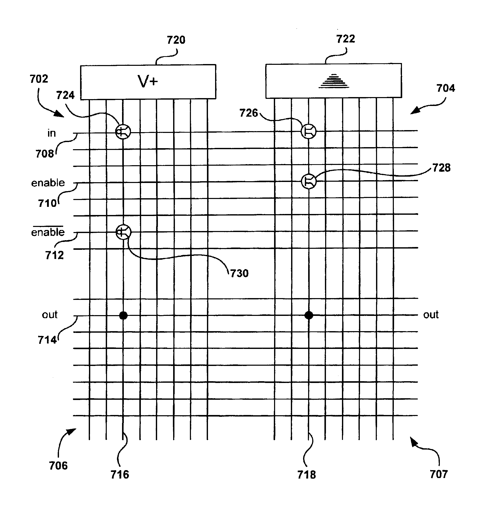
[0026]As discussed below, molecular-junction-nanowire crossbars represent one of a number of emerging nanoscale electronic circuit configuration media that can be used to construct nanoscale electronic circuits. Various techniques have been developed to selectively configure different types of electronic components, such as transistors, resistors, diodes, and conductions, at the junctions between the conductive paths at two different layers of a molecular-junction-nanowire crossbar. The present invention provides methods for configuring more complex, familiar electronic circuits using selective configuration of simple electronic components within molecular-junction-nanowire crossbars. In a first subsection, below, molecular-junction-nanowire crossbars are described. In a second subsection, a number of embodiments of the present invention that employ molecular-junction-nanowire-crossbar technology are described.

Molecular-Junction-Nanowire Crossbars

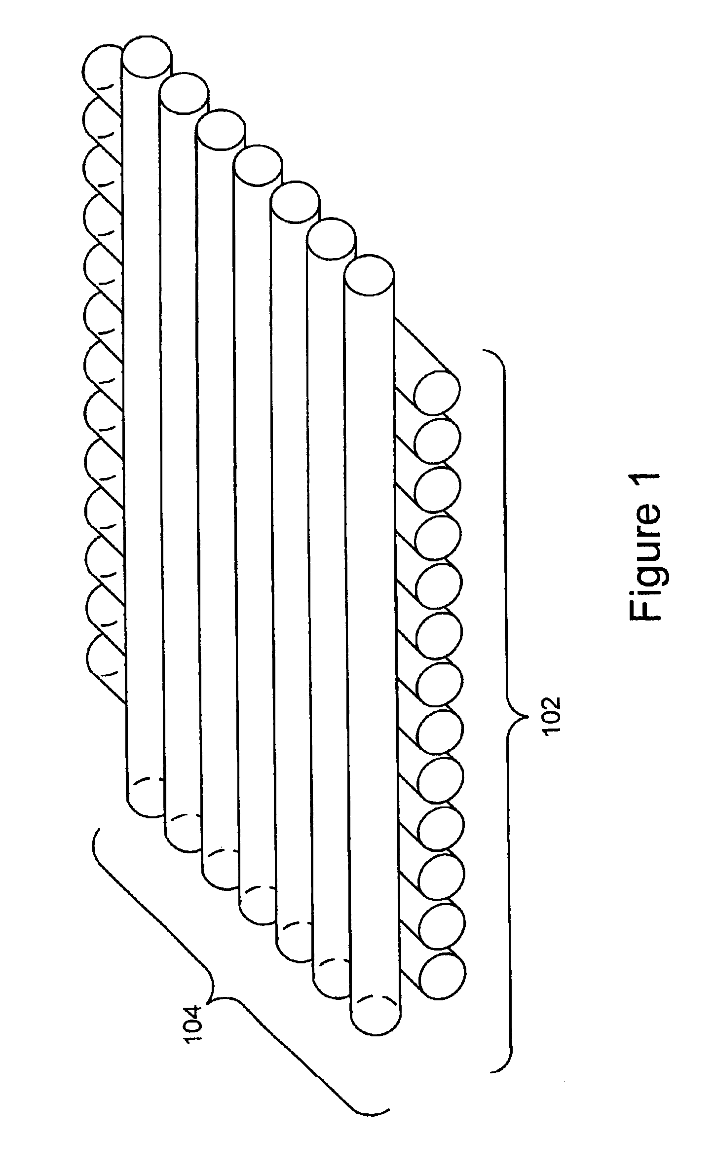
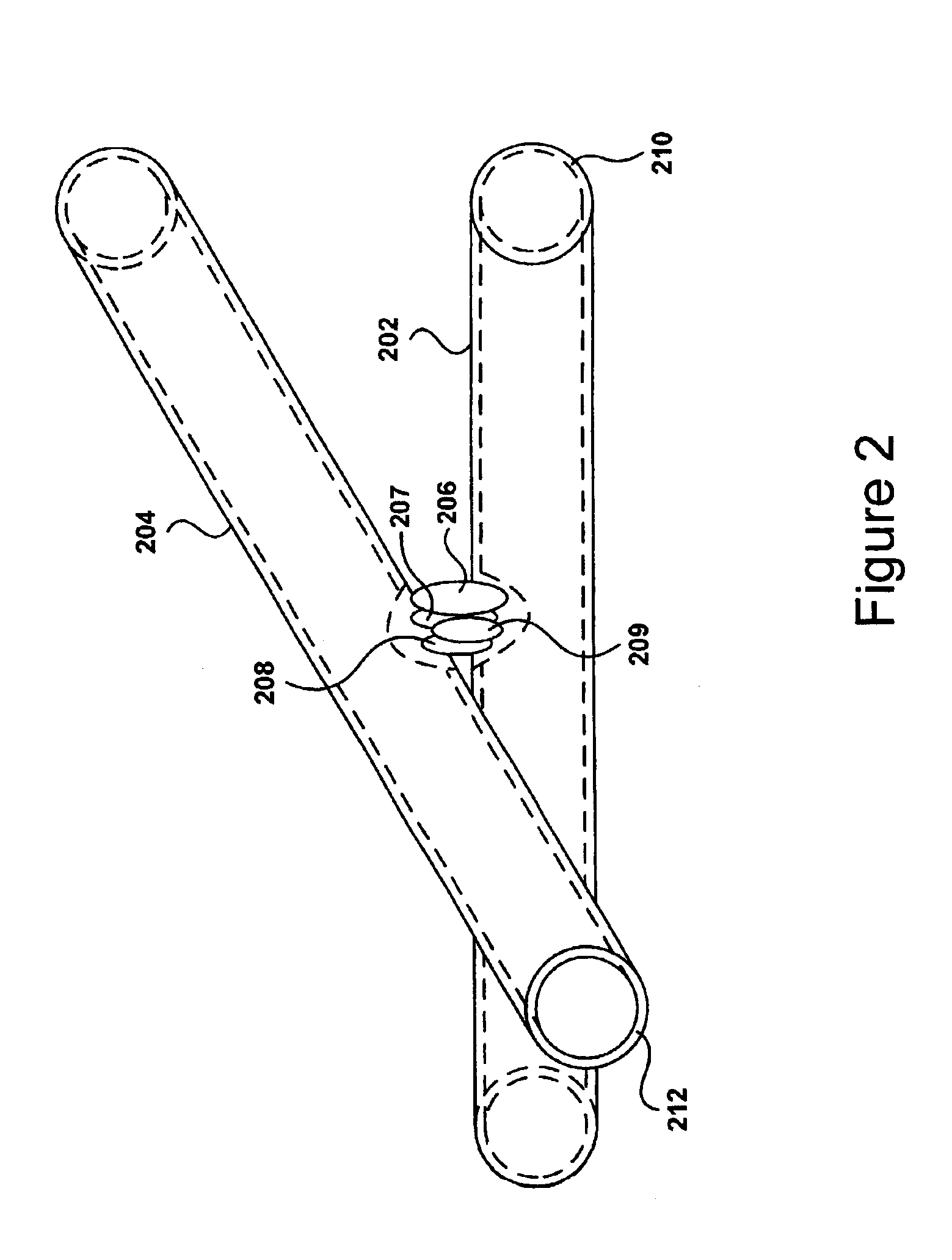
[0027]A relatively new and promising...


PUM


Abstract

Methods for implementing familiar electronic circuits at nanoscale sizes using molecular-junction-nanowire crossbars, and nanoscale electronic circuits produced by the methods. In one embodiment of the present invention, a 3-state inverter is implemented. In a second embodiment of the present invention, two 3-state inverter circuits are combined to produce a transparent latch. The 3-state inverter circuit and transparent-latch circuit can then be used as a basis for constructing additional circuitry, including master/slave flip-flops, a transparent latch with asynchronous preset, a transparent latch with asynchronous clear, and a master/slave flip-flop with asynchronous preset. 3-state inverters can thus be used to compose latches and flip-flops, and latches and flip-flops can be used, along with additional Boolean circuitry, to compose a wide variety of useful, state-maintaining circuits, all implementable within molecular-junction-nanowire crossbars by selectively configuring junctions within the molecular-junction-nanowire crossbars.

Description

TECHNICAL FIELD[0001]The present invention relates to electrical circuitry and, in particular, to programmanble, nanoscale-sized electrical circuits, including latches and flip-flops, configured from molecular-junction-nanowire crossbars that may be integrated with additional components in extremely dense electrical subsystems.BACKGROUND OF THE INVENTION[0002]During the past fifty years, the electronics and computing industries have been relentlessly propelled forward by the ever decreasing sizes of basic electronic components, such as transistors and signal lines, and by the correspondingly ever increasing component densities of integrated circuits, including processors and electronic memory chips. Eventually, however, it is expected that fundamental component-size limits will be reached in semiconductor-circuit-fabrication technologies based on photolithographic methods. As the size of components decreases below the resolution limit of ultraviolet light, for example, far more tech...

Claims


Application Information

Patent Timeline
Patent Type & Authority Patents(United States)
IPC IPC(8): G11C13/02H01L27/28H01L51/05H01L51/30H01L51/00
CPCB82Y10/00G11C13/0014G11C13/02G11C2213/77G11C2213/81H01L27/28H01L51/0048H01L51/0052H01L51/0595Y10S977/94H10K85/221H10K85/615H10K10/701H10K19/00
Inventor SNIDER, GREG
Owner HEWLETT PACKARD DEV CO LP
Why Eureka
Try Eureka