

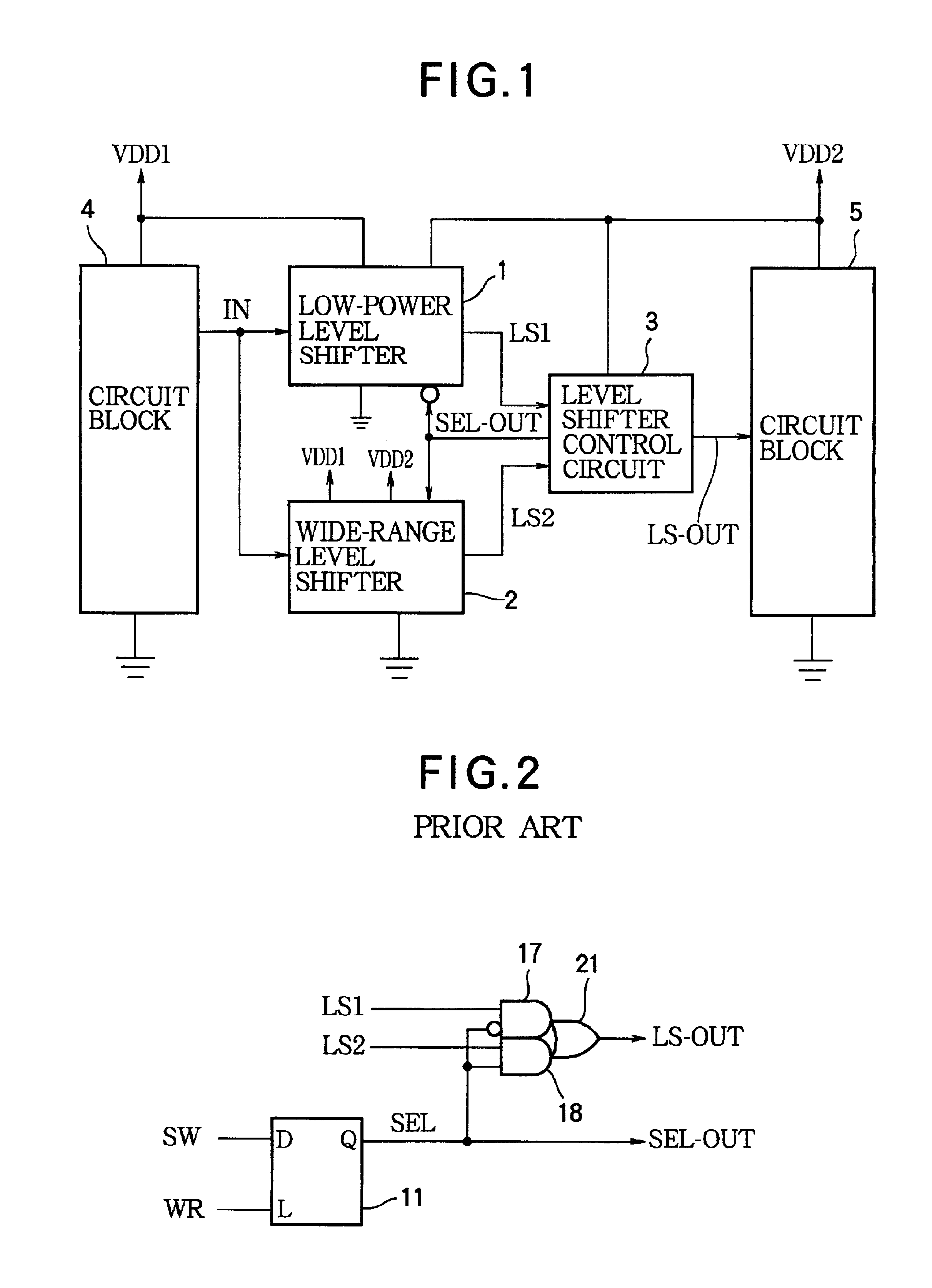
Level shifter control circuit with delayed switchover to low-power level shifter
a level shifter and control circuit technology, applied in logic circuit coupling/interface arrangement, pulse technique, instruments, etc., can solve the problems of low-power level shifter initially inability to operate, large current consumption during signal transition,
- Summary
- Abstract
- Description
- Claims
- Application Information
AI Technical Summary
Benefits of technology
Problems solved by technology
Method used
Image

Examples
first embodiment
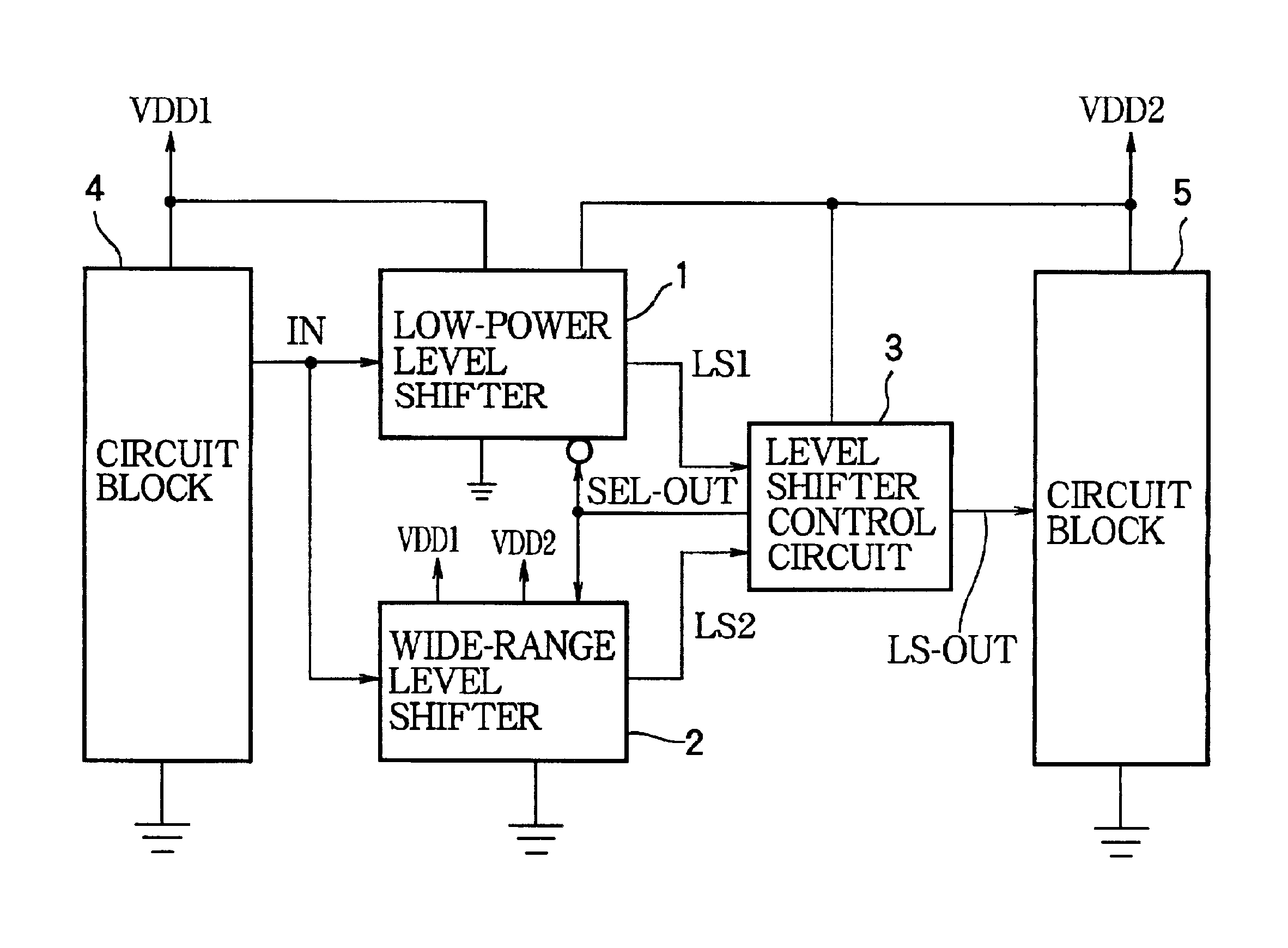
[0044]As the invention, FIG. 6 shows a level shifter control circuit comprising a register 11, a D-type flip-flop circuit 12, a counter circuit 13, a delay circuit 14, AND gates 16, 17, 18, and OR gates 19, 20, 21. The input signals to this level shifter control circuit are the output signal LS1 of the low-power level shifter 1 (when selected), the output signal LS2 of the wide-range level shifter 2 (when selected), the switching signal SW and write signal WR described above, a time-base clock signal TBCLK, and a system reset signal RST. The time-base clock signal is, for example, a comparatively low-frequency oscillator signal used as a time base for a real-time clock function, or more generally any signal that alternates between the high and low logic levels at regular intervals. The time-base clock signal, the system reset signal, and the selection signals SW and WR are generated by, for example, other functional blocks in the integrated circuit of which the level shifter control...
second embodiment
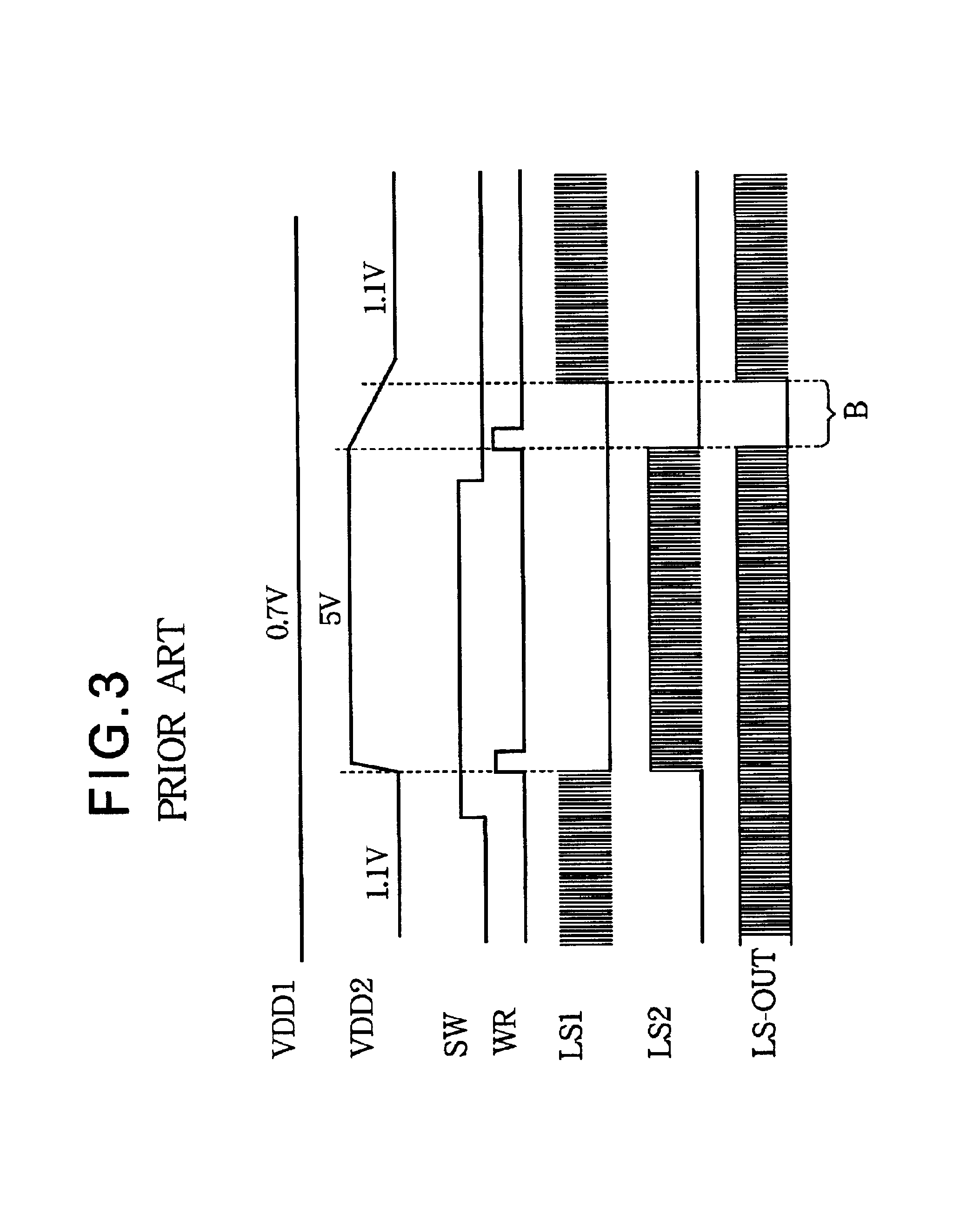
[0068]The operation of the second embodiment will be described with reference to the timing diagram in FIG. 9, which shows waveforms of the system reset signal RST, switching signal SW, write signal WR, selection signal SEL, output selection signal SEL-OUT, delayed selection signal DSEL, integrated voltage signal INT, inverted signal INV, and internal reset signal IRST. Waveforms of the power supply voltages VDD1, VDD2 are omitted since they are the same as in FIG. 7; that is, VDD1 remains constant at 0.7 volts, while VDD2 is initially 1.1 volts, then rises to five volts, then returns to 1.1 volts.
[0069]At power-up or a system reset, the system reset signal RST and internal reset signal IRST go high, resetting the D-type flip-flop circuit 12, so the delayed selection signal DSEL is low. The output of inverter 31 is therefore high, PMOS transistor 33 is in the off-state, and NMOS transistor 34 is in the on-state, holding the integrated voltage signal INT at the low level and the inve...
third embodiment
[0077]As the invention, FIG. 10 shows a level shifter control circuit comprising a register 11, AND gates 17, 18, OR gates 20, 21, another register 41, and a microcontroller unit (MCU) 42. Detailed descriptions of the register 11, and the AND and OR gates will be omitted, as they are identical to the corresponding elements in the preceding embodiments.
[0078]The register 41 is similar to the register 11, having a data input terminal (D), a latch clock input terminal (L), and an output terminal (Q). The data input terminal receives a delayed switching signal DSW. The latch clock input terminal receives a delayed write signal DWR. A delayed selection signal DSEL is supplied from the output terminal to OR gate 20.
[0079]The MCU 42 comprises, for example, a central processing unit and memory, the memory storing a program which is executed by the central processing unit to carry out embedded control functions in some type of electronic device. The term ‘microcontroller’ is often used to de...
PUM
 Abstract
Description
Claims
Application Information