ASIC architecture for active-compensation of a programmable impedance I/O

a technology of programmable impedance and asic architecture, which is applied in the direction of logic circuit coupling/interface arrangement, pulse technique, instruments, etc., can solve the problems of time-consuming and costly custom circuit design, test, verification and characterization of i/o, and the design of dynamically controlled and programmable impedance drivers

Inactive Publication Date: 2005-07-26
IBM CORP
View PDF11 Cites 9 Cited by
  • Summary
  • Abstract
  • Description
  • Claims
  • Application Information

AI Technical Summary

Benefits of technology

[0011]The preferred embodiment of the invention uses a circuit architecture for a circuit that provides an actively compensated and programmable impedance I/O that meets Application Specific Integrated Circuit (ASIC) methodology requirements and provides all the advantages of a custom circuit design. This architecture all

Problems solved by technology

The design of such dynamically-controlled and programmable impedance drivers is often quite complex compared to I/O cell designs withou

Method used


Image

  • ASIC architecture for active-compensation of a programmable impedance I/O
  • ASIC architecture for active-compensation of a programmable impedance I/O
  • ASIC architecture for active-compensation of a programmable impedance I/O

Examples


Embodiment Construction

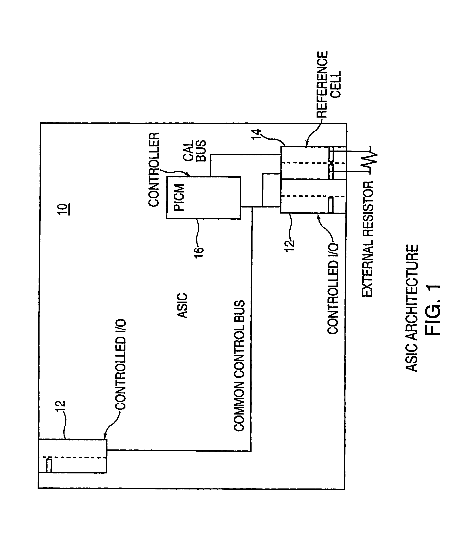
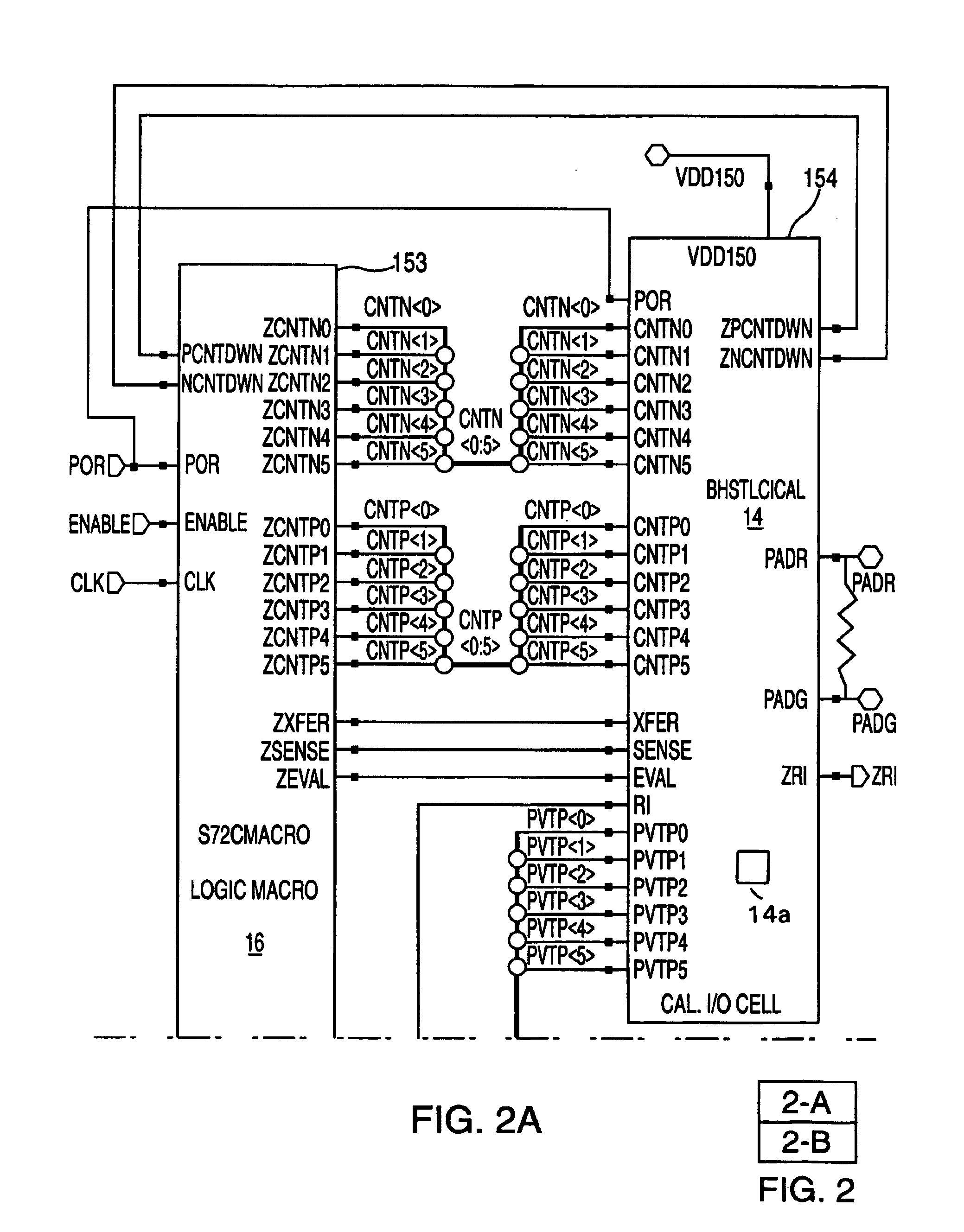
[0022]FIG. 1 shows a circuit architecture 10 generally comprising I / O cell 12 that is being controlled, reference cell 14, and digital controller 16. FIG. 2 is a more detailed block diagram of architecture 10 showing all the input and output signal names.

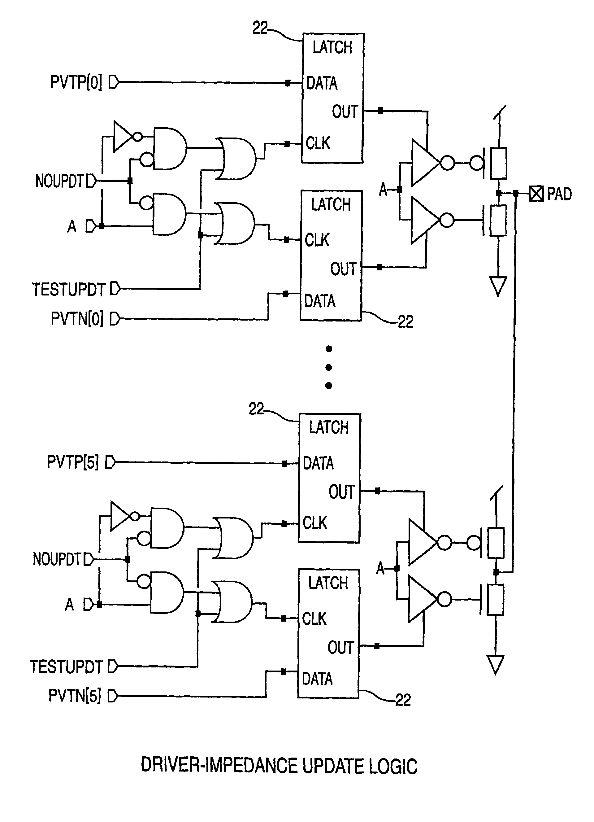
[0023]The I / O cell 12, shown in detail in FIG. 3, may be a typical high speed I / O with the addition of N number of control bits for pull-up and pull-down control of the driver Impedance. The I / O cell also has three additional control inputs PNDRIVE, NOUPDT and TESTUDT all of which come from the digital controller. A typical driver would pass data from an internal pin “A” and drive the data at the output pin “PAD” with a fixed driver impedance for both pull-up and pull-down. In the disclosed I / O cell, the driver impedance depends on the PFET, schematically represented at 12a in FIG. 2B, control bits (PVTP[5:0]) and NFET control bits (PVTN[5:0]). The input “PNDRIVE” enables a default maximum value of driver impedance to be maintained....


PUM


Abstract

A method of, and a circuit for, impedance control. The method comprises the steps of providing an input/output cell having a controllable input/output impedance, providing a reference cell including a node having a variable voltage, and comparing the voltage of the node to a reference voltage. The voltage of the node is adjusted during a defined period and according to a defined procedure, and during that defined period, a digital signal is generated. That digital signal is transmitted to the input/output cell to adjust the input/output impedance. Preferably, the circuit is embodied as a digital controller designed as a synthesized core or macro. The advantage of this implementation is that it never has to be redesigned in future technologies. The digital controller may be carried over to future technologies in the form of VHDL code, which is pure logic and independent of technology.

Description

BACKGROUND OF THE INVENTION[0001]1. Field of the Invention[0002]This invention generally relates to I / O cells with programmable active input bias. More specifically, the invention relates to a circuit architecture, and to a method of using this circuit architecture, for an actively compensated and programmable impedance I / O.[0003]2. Prior Art[0004]CMOS I / O drivers require a tightly controlled driver impedance to maintain signal integrity when switched at high speeds. I / O drivers have been designed that maintain the driver's impedance by making adjustments for Integrated Circuit (IC) process variations, temperature and voltage changes. These I / O designs consist of a custom I / O circuit design and the overhead circuitry required to set the driver impedance for a given IC process; and then maintain this impedance when changes in temperature and voltage are sensed.[0005]The design of such dynamically-controlled and programmable impedance drivers is often quite complex compared to I / O cel...

Claims


Application Information

Patent Timeline
IPC IPC(8): H03K19/00G06F3/00H03K19/0175
CPCH03K19/0005
Inventor COUGHLIN, JR., TERRY C.WANG, GEOFFREY
Owner IBM CORP
Why Eureka
Try Eureka