Slurry for chemical mechanical polishing and method of manufacturing semiconductor device
a technology of chemical mechanical polishing and slurry, which is applied in the direction of polishing compositions, other chemical processes, manufacturing tools, etc., can solve the problems of uneven diameter, difficult to control erosion, scratching of wirings and interlayer insulating films,
- Summary
- Abstract
- Description
- Claims
- Application Information
AI Technical Summary
Benefits of technology
Problems solved by technology
Method used
Image

Examples
example 1
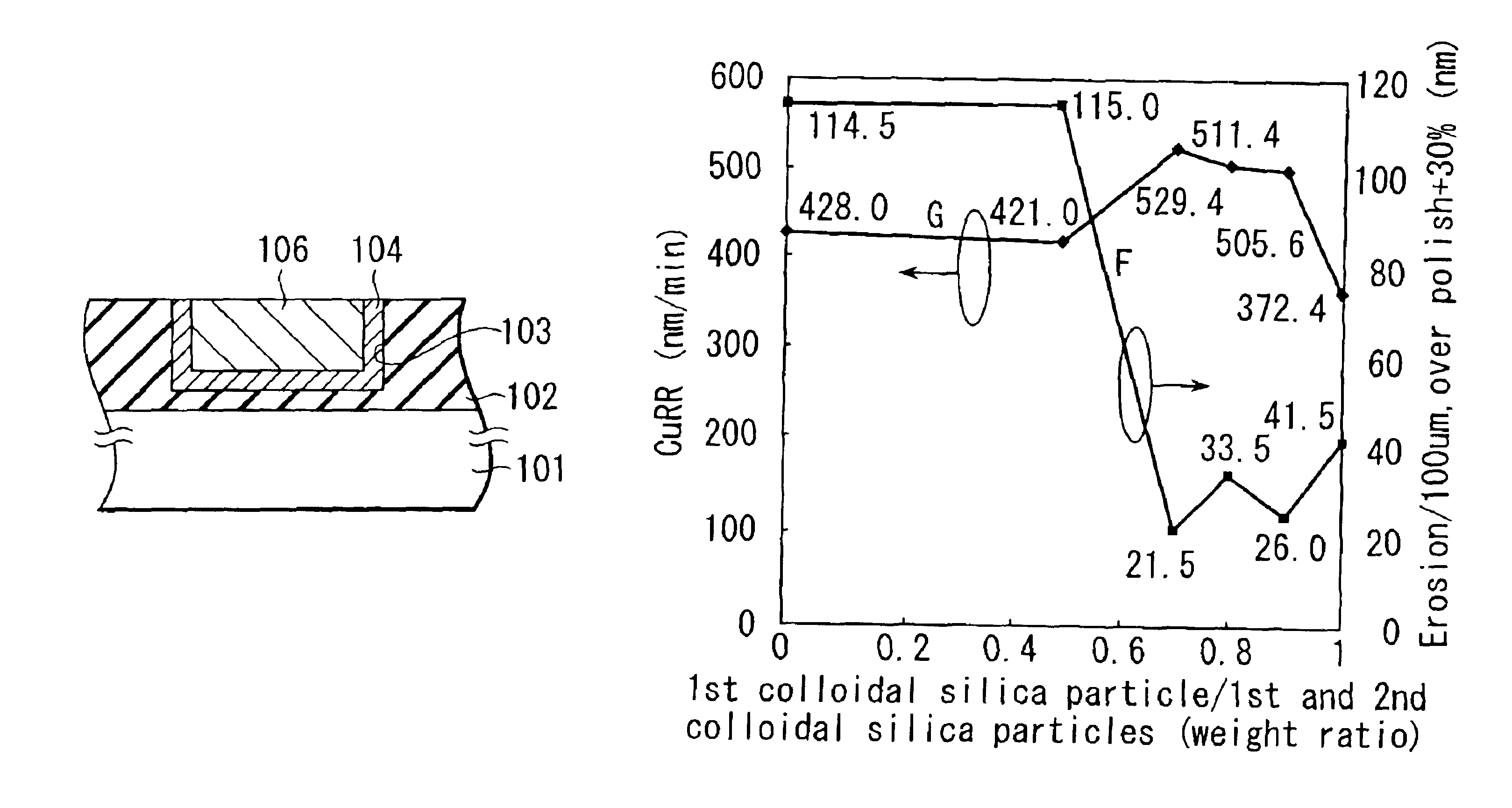
[0099]First of all, as shown in FIG. 5A, an insulating film 102 consisting of silicon oxide, for example, was formed on a silicon substrate (silicon wafer) 101 provided with a semiconductor element, for instance, and then, the surface of the insulating film 102 was flattened. Thereafter, this insulating film 102 was selectively etched to form a wiring groove 103 having a depth of 400 nm. Then, a TaN film 104 about 10 nm in thickness as a barrier film was deposited on the insulating film 102 as well as on the inner surface of the wiring groove 103. Thereafter, a Cu film 105 having a thickness of 800 nm was deposited on the TaN film 104 at first by means of sputtering method and then, by means of plating method.
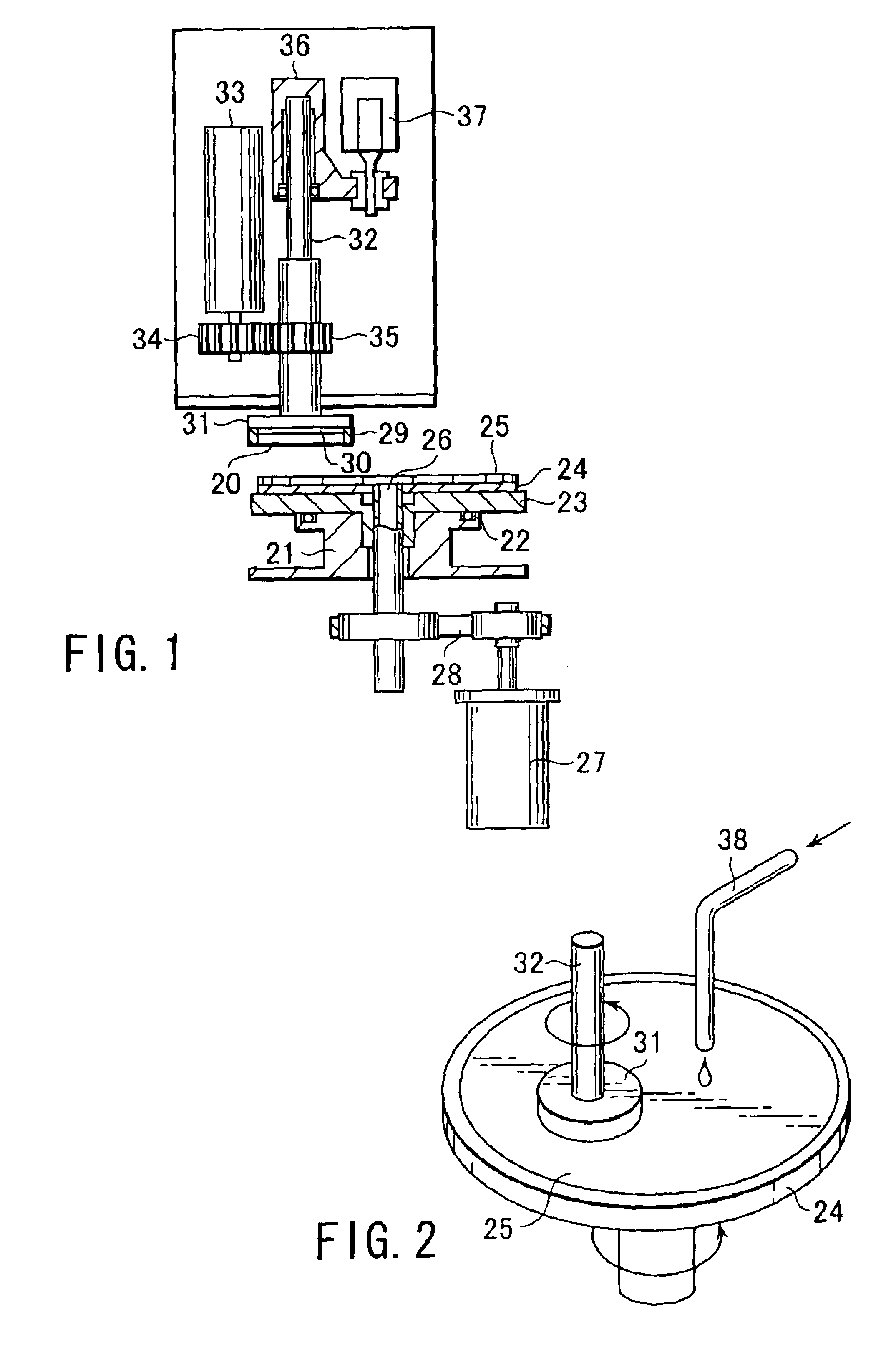
[0100]Then, the surface of the Cu film 105 was subjected to a CMP treatment by making use of the polishing apparatus shown in FIGS. 1 and 2 and a first CMP slurry having a composition shown below under the conditions as described below, thereby permitting the Cu film 105 to rem...
example 2
[0127]First of all, as shown in FIG. 8A, an insulating film 202 was formed on a silicon substrate (silicon wafer) 201 provided with a semiconductor element, for instance, and then, the insulating film 202 was selectively etched to form a wiring groove 203 having a depth of 400 nm. This insulating film 202 was formed of a Low-K insulating film which was soft, brittle and easily peelable such as an organic film or a porous film. Then, a Nb film 204 about 15 nm in thickness as a barrier film was deposited on the insulating film 202 as well as on the inner surface of the wiring groove 203. Thereafter, an Al film 205 having a thickness of 800 nm was deposited on the Nb film 204 by means of sputtering method.
[0128]Then, the surface of the Al film 205 was subjected to a CMP treatment by making use of the polishing apparatus shown in FIGS. 1 and 2 and a first CMP slurry having a composition shown below under the conditions as described below, thereby permitting the Al film 205 to remain onl...
example 3
[0152]A semiconductor device was manufactured by burying a Cu wiring (damascene wiring) in a wiring groove with a TaN film being interposed therebetween according to the same procedures as explained in Example 1, except that a Cu film which was deposited on a silicon oxide insulating film formed on a silicon substrate (silicon wafer) provided with a semiconductor element, for example, was subjected to a CMP treatment by making use of the polishing apparatus shown in FIGS. 1 and 2 and a CMP slurry having a composition shown below under the conditions as described below.
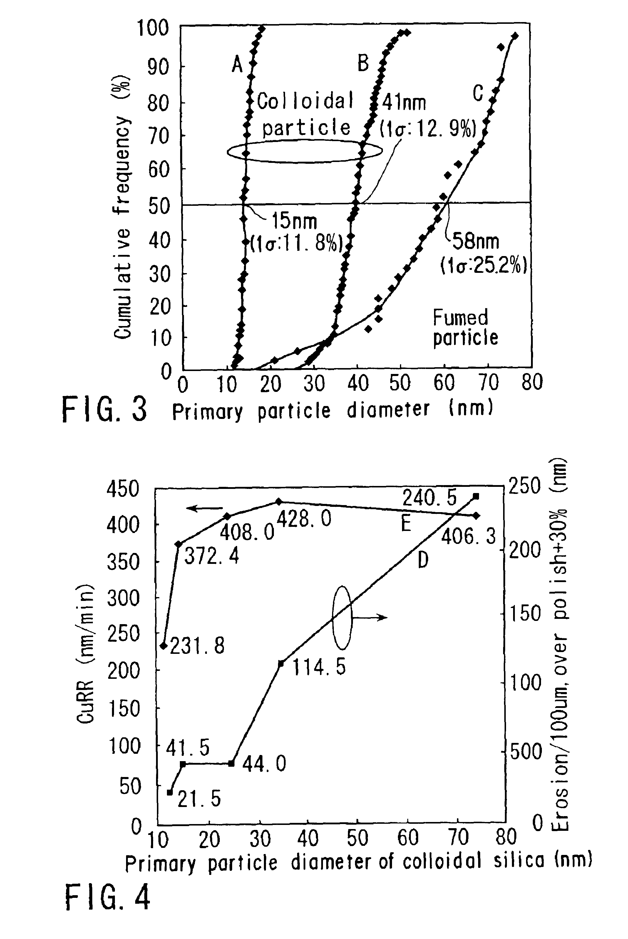
[0153]Polishing particles: Colloidal silica particles differing in the degree of association and having a primary particle diameter of 25 nm accounts for 1.0% by weight;
[0154]Ammonium persulfate (oxidizing agent) accounts for 1% by weight;
[0155]Quinaldinic acid (oxidation inhibitor) accounts for 0.5% by weight;
[0156]Potassium dodecylbenzene sulfonate accounts for 0.06% by weight;
[0157]pH=9.2 (adjusted by adding an aque...
PUM
 Abstract
Description
Claims
Application Information
 - R&D
- Intellectual Property
- Life Sciences
- Materials
- Tech Scout
- Unparalleled Data Quality
- Higher Quality Content
- 60% Fewer Hallucinations
Browse by: Latest US Patents, China's latest patents, Technical Efficacy Thesaurus, Application Domain, Technology Topic, Popular Technical Reports.
© 2025 PatSnap. All rights reserved.Legal|Privacy policy|Modern Slavery Act Transparency Statement|Sitemap|About US| Contact US: help@patsnap.com