Unlock instant, AI-driven research and patent intelligence for your innovation.

Circuit design method and computer program product

a technology of circuit design and computer program, applied in computer aided design, instruments, computing, etc., can solve the problems of large processing time and complex design of lsi (large scale integration), and achieve the effect of reducing the design tim

Inactive Publication Date: 2005-08-09
FUJITSU LTD
View PDF2 Cites 10 Cited by
  • Summary
  • Abstract
  • Description
  • Claims
  • Application Information

AI Technical Summary

Benefits of technology

[0007]An object of the present invention is to provide a circuit design technology for efficiently adjusting circuit timing in a short TAT.
[0009]With this constitution, since the variable delay cell is inserted into a circuit in advance, and the delay in the variable delay cell can be corrected when a timing error is generated, it is not necessary to change cells other than the variable delay cell, and external routing. Consequently, the timing for a circuit is adjusted efficiently in a short period, and thus the design time can be reduced.

Problems solved by technology

As a scale increase, a speed increase, and miniaturization of a semiconductor chip advance, LSI (Large Scale Integration) design is getting complicated.
Since adjusting (correcting) the timing during LSI development requires a large amount of processing time since a layout process is conducted again after the timing is adjusted.
Also, since the layout process is repeated, cell placement and routing change slightly, and consequently, a problem such as a new timing error occurs.

Method used


Image

  • Circuit design method and computer program product
  • Circuit design method and computer program product
  • Circuit design method and computer program product

Examples


Embodiment Construction

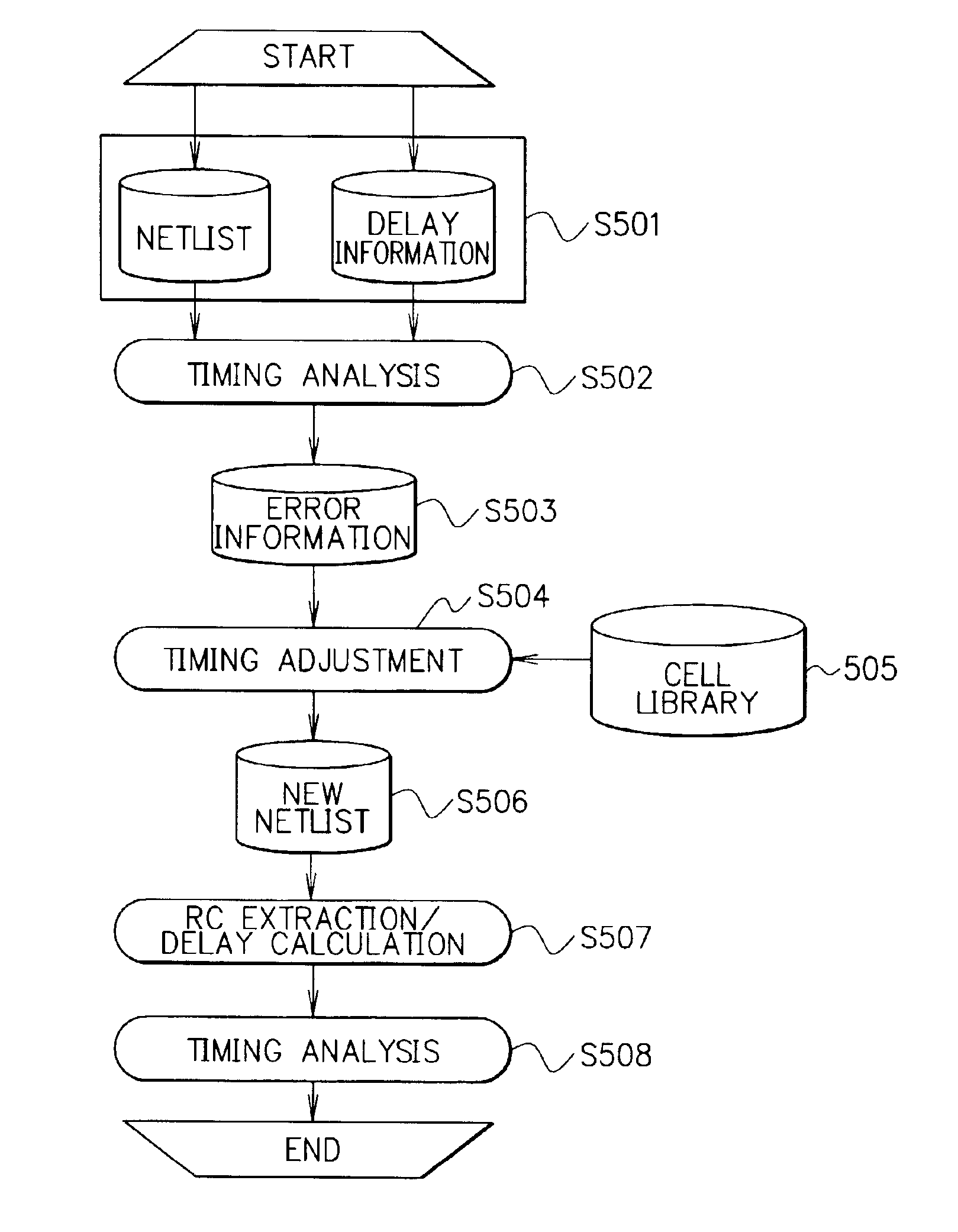
[0016]FIG. 1 is a circuit diagram of an integrated circuit describing an integrated circuit design method according to an embodiment of the present invention. This integrated circuit is formed as a semiconductor chip. The integrated circuit includes a large number of D type flip-flops (simply referred to as a flip-flop hereafter) 103 and 113. The flip-flops 103 and 113 are logic circuits, and supply a datum from an output terminal Q based on an input datum entered on an input terminal D in sync with a clock signal on a clock terminal CLK.

[0017]A clock signal is supplied for a clock input terminal CLK0. Then, the clock signal is supplied for the clock terminal CLK of a large number of the flip-flops 103 through a variable delay cell 101 and a buffer102. The clock signal on the clock input terminal CLK0 is also supplied for the clock terminal CLK of a large number of the flip-flops 113 through a buffer 111, a variable delay cell 112, and a logical addition (AND) circuit 114.

[0018]The ...


PUM


Abstract

A circuit design technology which can facilitate timing adjustment for a circuit whose layout has been designed. The circuit design method including the steps of entering design data for a circuit including a variable delay cell inserted in advance at a part where delay adjustment is expected necessary in terms of a circuit characteristic during an initial layout, analyzing timing of the entered design data, and correcting the delay in the variable delay cell when an error occurs as a result of the timing analysis.

Description

CROSS-REFERENCE TO RELATED APPLICATIONS[0001]This application is based upon and claims the benefit of priority from the prior Japanese Patent Application No. 2002-072736, filed on Mar. 15, 2002, the entire contents of which are incorporated herein by reference.BACKGROUND OF THE INVENTION[0002]1. Field of the Invention[0003]The present invention relates to a circuit design technology, and specifically relates to a circuit design technology for facilitating timing adjustment for a circuit whose layout has been designed.[0004]2. Description of the Related Art[0005]As a scale increase, a speed increase, and miniaturization of a semiconductor chip advance, LSI (Large Scale Integration) design is getting complicated. In addition, recently, importance of adapting to DFT (Design For Test), adapting to increasing complexity of clock circuit due to insertion of a gated clock cell for decreasing power consumption, and fine-tuning timing in an interface (I / F) with an external DRAM circuit is in...

Claims


Application Information

Patent Timeline
Patent Type & Authority Patents(United States)
IPC IPC(8): G06F17/50H01L21/70H01L21/82H03K5/13
CPCG06F17/5031G06F17/5081G06F2217/84G06F30/3312G06F2119/12G06F30/398
Inventor MATSUMOTO, SHO
Owner FUJITSU LTD
Features
  • R&D
  • Intellectual Property
  • Life Sciences
  • Materials
  • Tech Scout
  • Unparalleled Data Quality
  • Higher Quality Content
  • 60% Fewer Hallucinations
Learn More