Method of forming an electronic device on a recess in the surface of a thin film of silicon etched to a precise thickness

a thin film, precise technology, applied in the direction of basic electric elements, semiconductor devices, electrical equipment, etc., can solve the problems of large problems such as and the inability to accurately measure the thickness of the surface of the thin film

Inactive Publication Date: 2005-08-16
INTELLECTUAL DISCOVERY INC
View PDF16 Cites 60 Cited by
  • Summary
  • Abstract
  • Description
  • Claims
  • Application Information

AI Technical Summary

Benefits of technology

[0009]An object of this invention is to provide a method of forming a precision recessed gate structure using selective Reactive Ion Etching (RIE) of regions in the silicon.
[0010]In accordance with this invention, a method is provided for forming precision recessed structure such as a gate structure by the process of forming an amorphized region in a SOI silicon layer by ion implantation into the too surface of the SOI silicon layer. The following step is selective Reactive Ion Etching (RIE) of the amorphized region in the silicon to form the recess therein.

Problems solved by technology

Scaling of SOI devices can be limited by the ability to thin the silicon.
This is a significant problem because source / drain contact resistance increases very rapid as the silicide layer approaches the BOX layer.
The method of FIGS. 1A and 1B has significant issues with the selective epitaxy necessary to form the raised source drain.
This process is difficult to control because it relies on the balance between silicon deposition and etching in a chemical vapor deposition reactor.
This leads to faceting of these edges resulting in unacceptable device structures.
The process is also very sensitive to surface contamination and prior processing conditions during such commonly used process steps as ion implantation, reactive ion etching and wet chemical cleans and etches.
This can lead to different deposition thicknesses on nFETs and pFETs which is generally undesirable.
This LOCOS recessing process is problematic due to the control necessary in defining the silicon thickness below the gate electrode stack.

Method used


Image

  • Method of forming an electronic device on a recess in the surface of a thin film of silicon etched to a precise thickness
  • Method of forming an electronic device on a recess in the surface of a thin film of silicon etched to a precise thickness
  • Method of forming an electronic device on a recess in the surface of a thin film of silicon etched to a precise thickness

Examples


Embodiment Construction

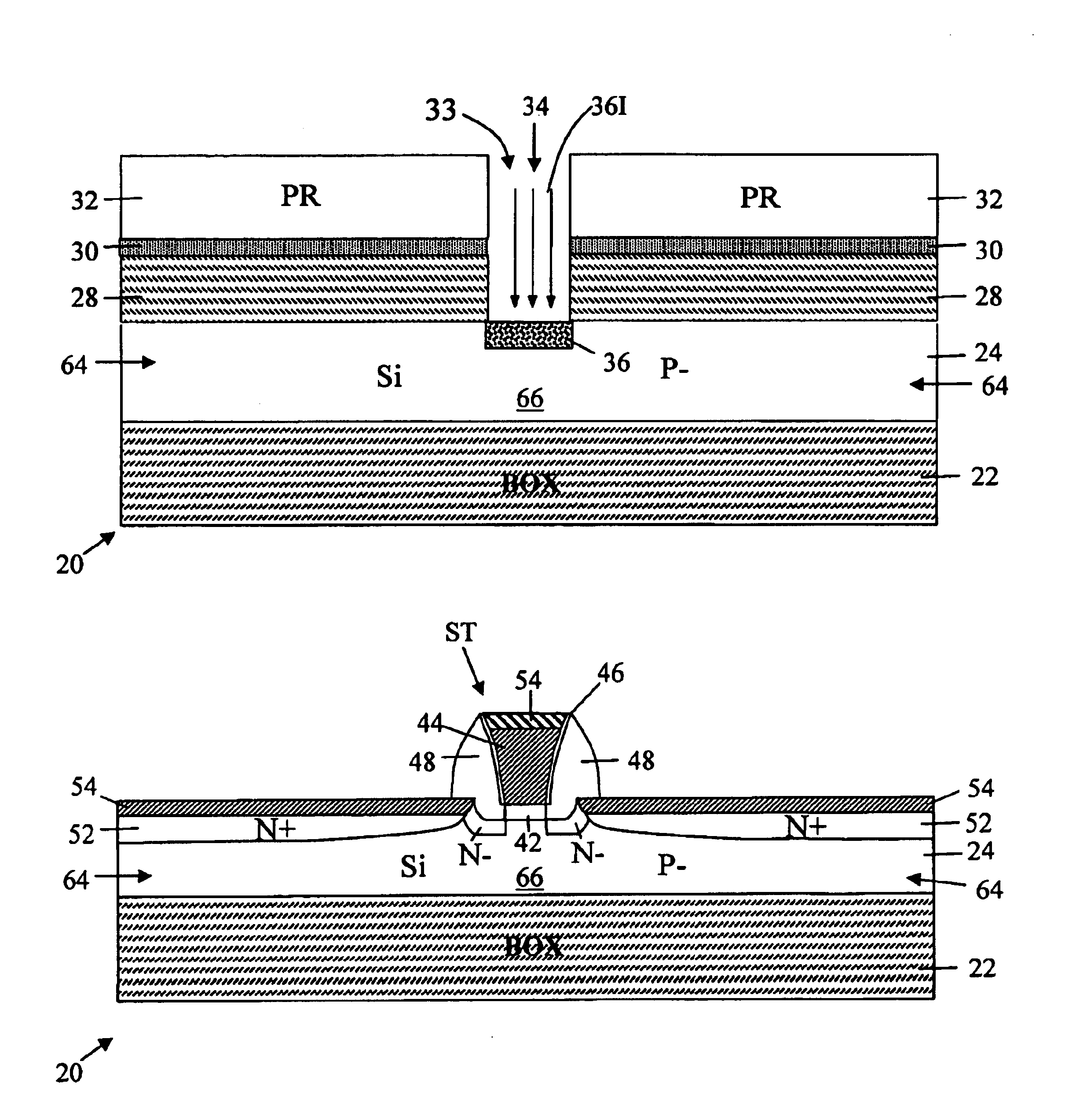
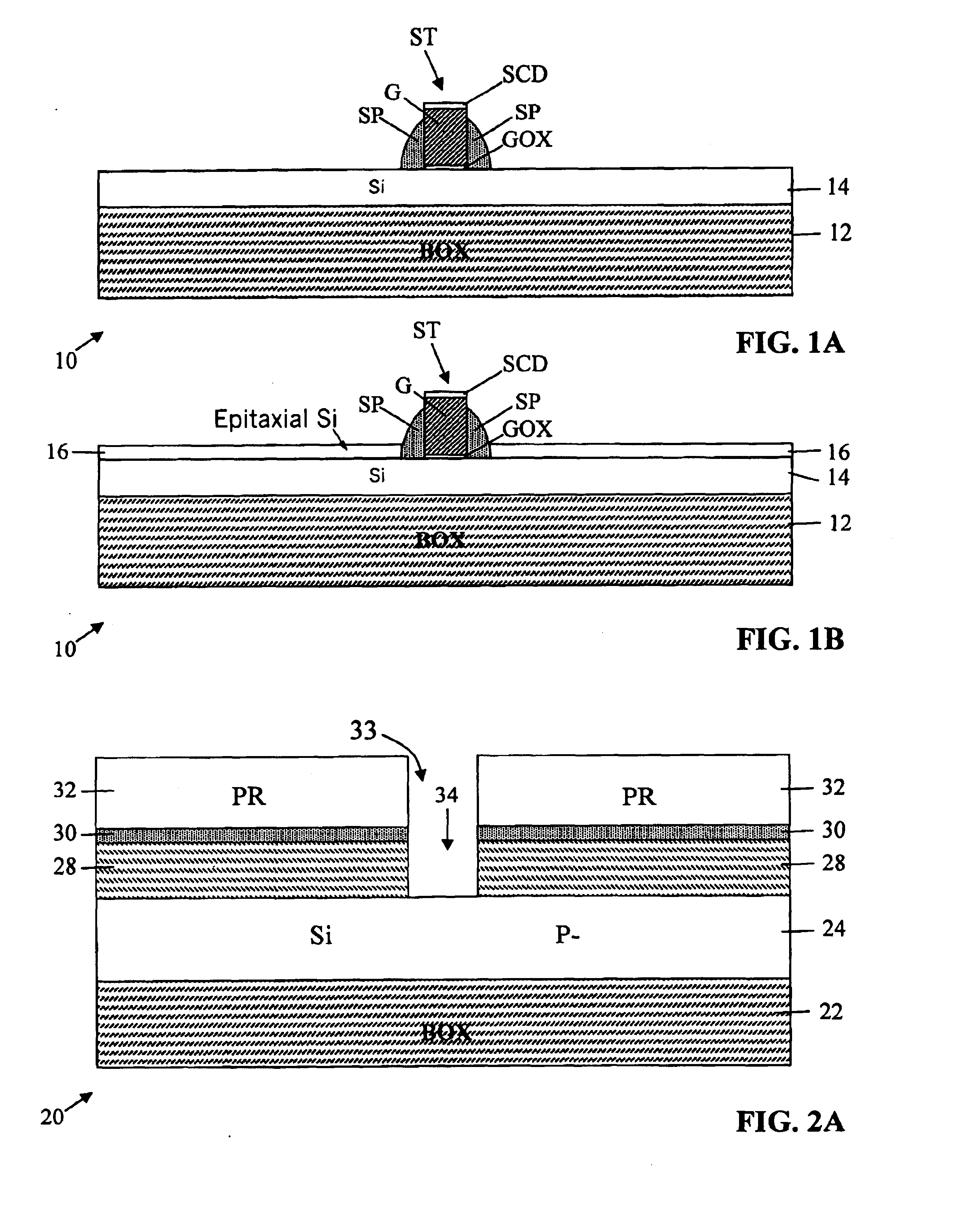
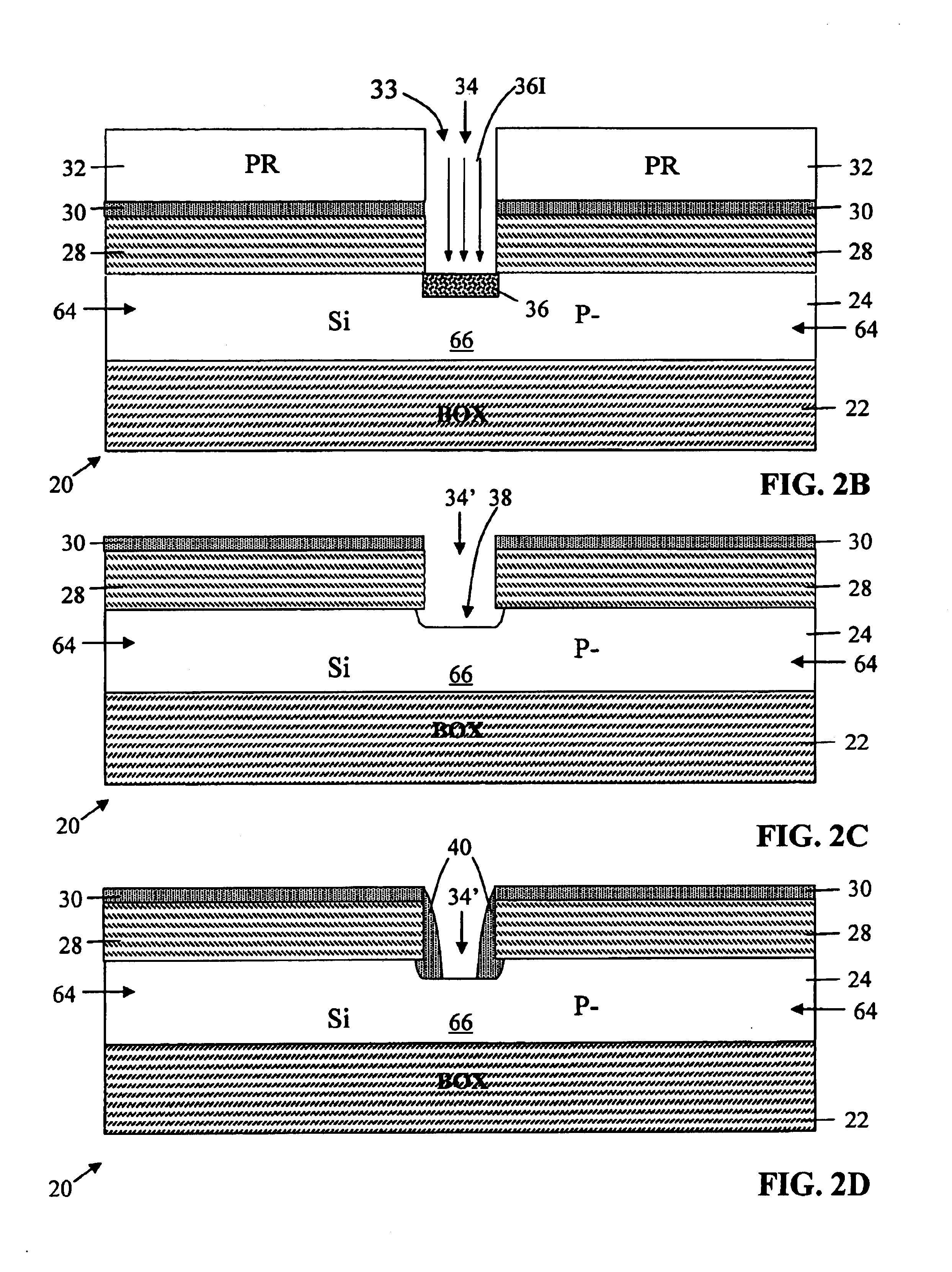
[0015]The process flow of one embodiment of this invention, which is employed to form a recessed gate MOSFET is described below with reference to FIGS. 2A-2M. In accordance with the method of FIGS. 2A-2M, the structure of an MOSFET device 20 is defined in part by production of a precisely controlled gate recess 38 shown in FIG. 2C formed by the selective reactive ion etching of amorphized silicon formed by ion implantation.

Form Masking Layers Over Silicon-on-Insulator (SOI) Layer

[0016]Starting in FIG. 2A, the MOSFET device 20 is shown in an early stage of manufacture. The substrate which has a planar upper surface comprises a BOX layer 22 formed on a wafer (not shown for convenience of illustration). Above the BOX layer 22, a conformal, planar, thin, p-doped, crystalline silicon layer 24 with top and bottom surfaces has been formed to serve as the doped region in which the source / drain and channel of an FET device is to be formed. As will be well understood by those skilled in the a...


PUM

PropertyMeasurementUnit
widthaaaaaaaaaa
thicknessaaaaaaaaaa
widthaaaaaaaaaa

Abstract

A method for precise thinning to form a recess to a precise depth in a crystalline silicon layer, which can be used to form various devices, such as MOSFET devices, includes the following steps. Form a patterning mask with a window therethrough over the top surface of the silicon layer. Form an amorphized region in the top surface of the silicon layer below the window. Selectively etch away the amorphized region of the silicon layer to form a recess in the surface of the silicon layer, and remove the patterning mask. In the case of an MOSFET device form a hard mask below the patterning mask with the window extending therethrough. Then create sidewall spacers in the window through the hard mask and form a gate electrode stack in the window. Then remove the hard mask and form the source/drain extensions, halos and regions plus silicide and complete the MOSFET device.

Description

BACKGROUND OF THE INVENTION[0001]This invention relates to methods of forming thinner silicon structures with precisely defined thicknesses in a thin silicon substrate, and more particularly to subtractive methods of precisely thinning selected portions of a silicon structure to form recesses with various precise depths in the surface of the thin silicon substrate into which recesses various devices including MOSFETS, resistors, capacitors and diodes can be formed.[0002]This invention provides a method for forming a structure with a precision recessed gate structure for an Ultra Thin (UT) Silicon-On-Insulator (SOI) device comprising a thin layer of doped silicon formed on the surface of a Buried OXide (BOX) layer. The method can also be used for precision thinning of selected regions of the top silicon layer on a SOI (SOI) wafer. This can be used to provide an optimal silicon thickness for each type of electronic device which is to be formed on the same wafer. For example, MOSFETS r...

Claims


Application Information

Patent Timeline
Patent Type & Authority Patents(United States)
IPC IPC(8): H01L21/02H01L21/336H01L29/78H01L29/66H01L21/3065H01L21/3213H01L21/265H01L21/28
CPCH01L21/3065H01L21/32137H01L29/66621H01L29/7834H01L21/26506H01L21/28114H01L29/665H01L29/6653H01L29/66553H01L21/2658
Inventor RAUSCH, WERNER A.WAGNER, TINA J.DESHPANDE, SADANAND V.
Owner INTELLECTUAL DISCOVERY INC
Why Eureka
Try Eureka