Pixel clock generation apparatus, pixel clock generation method, and image forming apparatus capable of correcting main scan dot position shift with a high degree of accuracy

a technology of pixel clock and image forming apparatus, which is applied in the direction of electrographic process apparatus, printing, instruments, etc., can solve the problems of exposure position shift, image quality degradation, and image quality degradation
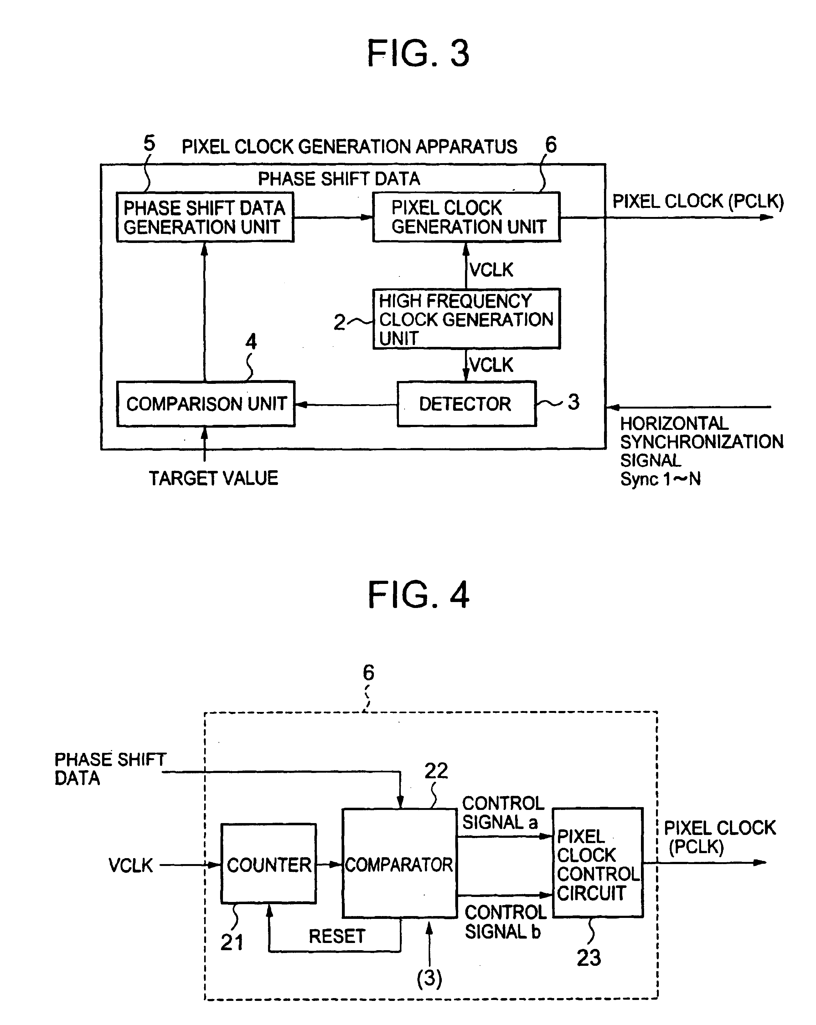
Inactive Publication Date: 2005-08-23
RICOH KK
View PDF14 Cites 64 Cited by
  • Summary
  • Abstract
  • Description
  • Claims
  • Application Information

AI Technical Summary

Benefits of technology

[0018]It is a general object of the present invention to provide an improved and useful pixel clock generation apparatus, pixel clock generation method, and image forming apparatus in which one or more of the above-mentioned problems are eliminated.

Problems solved by technology

The irregularity in the scan speed causes fluctuation in an image, which leads to degradation of image quality.
Further, in a multi-beam optical system that performs simultaneous scanning by using a plurality of light beams, if there is a difference among respective oscillation wavelengths of light emitting sources, an exposure position shift is generated in the case of an optical system in which chromatic aberration of a scan lens is not corrected.
Accordingly, a difference is generated among the scan widths of the optical spots, corresponding to the respective light emitting sources, in scanning a surface to be scanned, which causes degradation in image quality.
In the conventional method (frequency modulation method) of varying the frequency of the pixel clock, however, the configuration of the pixel clock controller is generally complex, and the complexity is increased as the frequency modulation range is decreased.
Therefore, there is a disadvantage in that realization of delicate control is not easy.
In addition, there is another disadvantage in that irregularity in the scan speed is generated by rotational jitter of the deflector and by expansion and contraction of the scan lens due to temperature variation, even in a light beam deflected by the same deflection (reflection) surface.
Further, there is a limit to control accuracy in the method of controlling the rotational motor of the deflector.
(1) The fθ characteristic of the scan lens is not sufficiently corrected.
Especially, it is impossible to avoid a main scan dot position shift due to environmental change even if optical tuning and electrical correction are conducted at the time of shipping the apparatus.
For example, even if there is no problem at the first printing, a problem can occur in that the hue of the first printing is different from that after a plurality of sheets of printing since the temperature in the apparatus is increased when printing out is performed successively.

Method used


Image

  • Pixel clock generation apparatus, pixel clock generation method, and image forming apparatus capable of correcting main scan dot position shift with a high degree of accuracy
  • Pixel clock generation apparatus, pixel clock generation method, and image forming apparatus capable of correcting main scan dot position shift with a high degree of accuracy
  • Pixel clock generation apparatus, pixel clock generation method, and image forming apparatus capable of correcting main scan dot position shift with a high degree of accuracy

Examples


embodiment 1

(Embodiment 1)

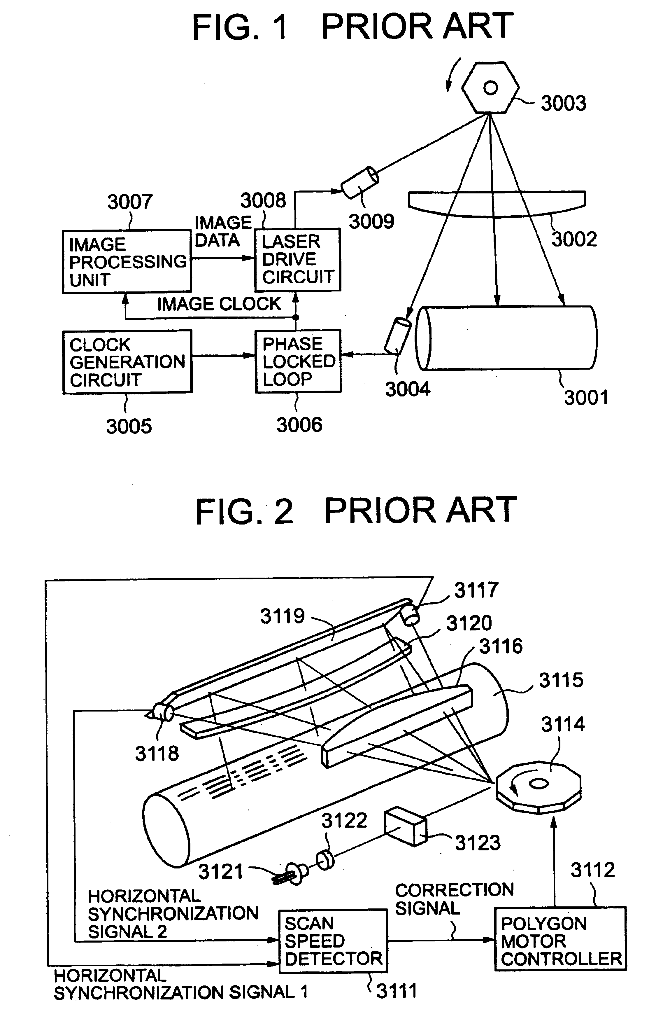
[0144]FIG. 11 is a schematic diagram of an image forming apparatus according to Embodiment 1 of the present invention. The image forming apparatus applies an electrophotography method. A laser light beam output from a semiconductor laser 100 is incident on a polygon mirror 103 as the deflector via a collimator lens 101 and a cylinder lens 102. The laser light beam deflected by the polygon mirror 103 passes through a fθ lens 104, which is a scan lens, and is reflected (partially transmitted) by a half mirror 105. Then, the laser light beam forms a light beam spot on the surface (surface to be scanned) of a photoconductor 106, which is a medium to be scanned, and forms an image (electrostatic latent image).

[0145]A photodetector (optical detection means) A 107 and a photodetector B 108 for generating the horizontal synchronization signals 1 and 2, respectively, are arranged at opposing ends of a surface to be detected. The surface to be detected possesses temporal correla...

embodiment 2

(Embodiment 2)

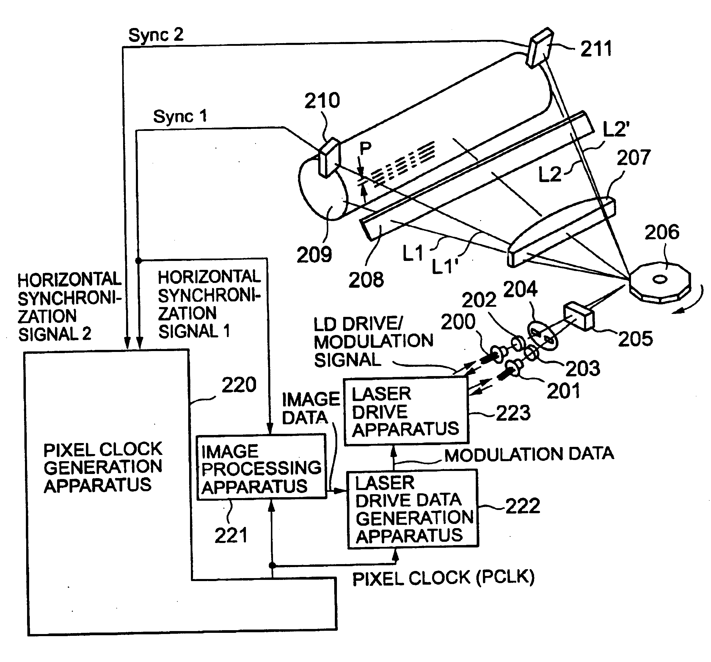
[0163]FIG. 16 is a schematic diagram of an image forming apparatus according to Embodiment 2 of the present invention. The image forming apparatus further includes a semiconductor laser 201 as a light beam source for reference for horizontal synchronization detection, in addition to the semiconductor laser 200 as the light beam source for image writing.

[0164]A laser light beam output from the semiconductor laser 200 for image writing is incident on a polygon mirror 206 via a collimator lens 202, a slit of an aperture 204, and a cylinder lens 205. The laser light beam deflected by the polygon mirror 206 forms a light beam spot on the surface (surface to be scanned) of a photoconductor 209 via a fθ lens 207 and a transparent member 208, and forms an electrostatic latent image.

[0165]The laser light beam output from the semiconductor laser 201 as the light beam source for reference is incident on the polygon mirror 206 via a collimator lens 203, a slit of the aperture 204,...

embodiment 3

(Embodiment 3)

[0173]FIG. 17 is a schematic diagram of an image forming apparatus according to Embodiment 3 of the present invention. In the image forming apparatus, a laser light beam output from a semiconductor laser 300 is incident on a polygon mirror 303 via a collimator lens 301 and a cylinder lens 302. The laser light beam deflected by the polygon mirror 303 passes through a fθ lens 304, is reflected by (partially transmitted through) a half mirror 305, forms a light beam spot on the surface (surface to be scanned) of a photoconductor 306, which is a medium to be scanned, via a toroidal lens 314, and forms an image (electrostatic latent image).

[0174]Photodetectors A 307, B 308, and C 309 for horizontal synchronization detection are arranged at the opposing ends and center of a surface to be detected, which is scanned by the laser light beam transmitted through the half mirror 5. That is, the horizontal synchronization detection means of this embodiment are configured such that ...


PUM


Abstract

A pixel clock generation apparatus includes a detector detecting a time interval between two horizontal synchronization signals. A comparing part compares the time interval detected by the detector and a target value, and outputs the difference. A phase shift data generation part stores one or more lookup tables each storing a pattern of phase shift data for controlling a phase shift amount of a pixel clock, and reads and outputs the phase shift data from the lookup table based on the difference that is output from the comparing part. A high frequency clock generation part generates a high frequency clock. A pixel clock generation part generates the pixel clock whose phase is controlled in accordance with the phase shift data based on the high frequency clock.

Description

BACKGROUND OF THE INVENTION[0001]1. Field of the Invention[0002]The present invention generally relates to image forming apparatuses such as laser printers, digital copying apparatuses, and the like, and more specifically, to an apparatus and method for generating a pixel clock used in theses image forming apparatuses.[0003]2. Description of the Related Art[0004]FIG. 1 shows a general structure of an image forming apparatus, such as a laser printer, a digital copying apparatus, and the like.[0005]In FIG. 1, a laser beam output from a semiconductor laser unit 3009 is scanned by a rotating polygon mirror 3003, forms an optical spot on a photoconductor 3001, which is a medium to be scanned, via a scan lens 3002, and forms an electrostatic latent image by exposing the photoconductor 3001. On this occasion, a photodetector 3004 detects the scan beam for each line. A phase locked loop 3006 receives a clock from a clock generation circuit 3005, generates a phase-locked image clock (pixel c...

Claims


Application Information

Patent Timeline
Patent Type & Authority Patents(United States)
IPC IPC(8): B41J2/435B41J2/47G03G15/043G03G15/30
CPCG03G15/043G03G15/305
Inventor OMORI, ATSUFUMIISHIDA, MASAAKINIHEI, YASUHIROOZASA, DAN
Owner RICOH KK
Why Eureka
Try Eureka