MOS type image pickup device having pixel interleaved array layout and one analog to digital conversion unit provided per each pair of adjacent photoelectric conversion columns

a photoelectric conversion column and pickup device technology, applied in the direction of radio frequency controlled devices, instruments, television systems, etc., can solve the problems of increasing manufacture costs, and achieve the effect of suppressing the increase in manufacture costs and improving the integration degree of photoelectric conversion elements

Inactive Publication Date: 2005-08-23
FUJIFILM CORP
View PDF16 Cites 57 Cited by
  • Summary
  • Abstract
  • Description
  • Claims
  • Application Information

AI Technical Summary

Benefits of technology

[0019]It is an object of the present invention to provide a MOS type solid state image pickup device with built-in A / D conversion units capable of facilitating to improve the integration degree of photoelectric conversion elements while an increase in the manufacture cost is suppressed.
[0021]By disposing a number of photoelectric conversion elements in the above manner, an effective integration degree of photoelectric conversion elements in a semiconductor substrate can be improved.
[0026]Alternatively, one output signal line is provided for each pair of adjacent photoelectric conversion element columns with positioning between the pair as viewed in plan, and one A / D conversion unit is provided for each output signal line. In this case, the number of output lines can be reduced.

Problems solved by technology

For example, if the integration degree of photoelectric conversion elements is set so that the pitch between photoelectric conversion elements in the photoelectric conversion element row direction becomes about 4 μm, highly sophisticated micro patterning techniques are required when AND conversion units are formed, and the manufacture cost increases.

Method used


Image

  • MOS type image pickup device having pixel interleaved array layout and one analog to digital conversion unit provided per each pair of adjacent photoelectric conversion columns
  • MOS type image pickup device having pixel interleaved array layout and one analog to digital conversion unit provided per each pair of adjacent photoelectric conversion columns
  • MOS type image pickup device having pixel interleaved array layout and one analog to digital conversion unit provided per each pair of adjacent photoelectric conversion columns

Examples


first embodiment

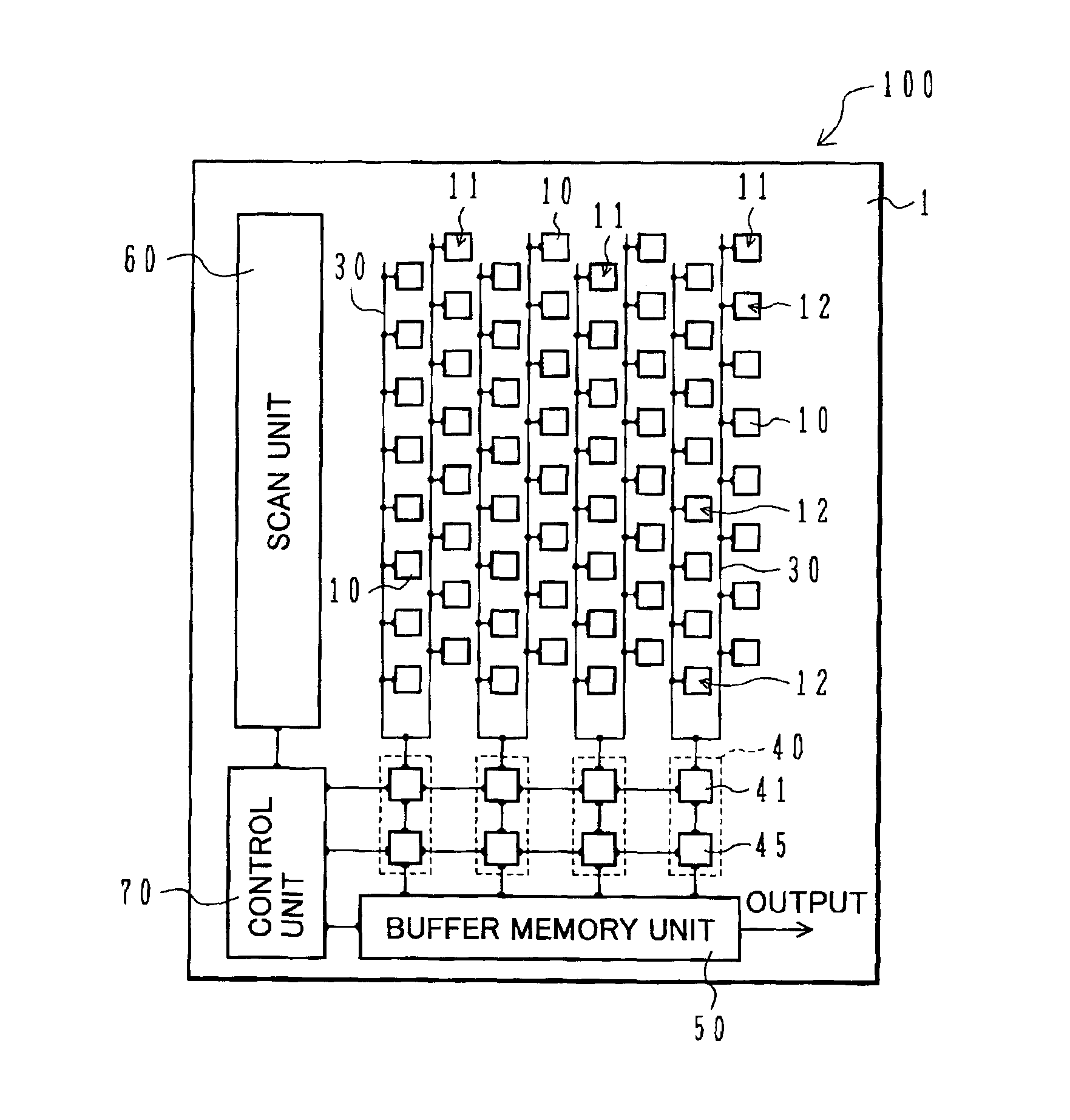
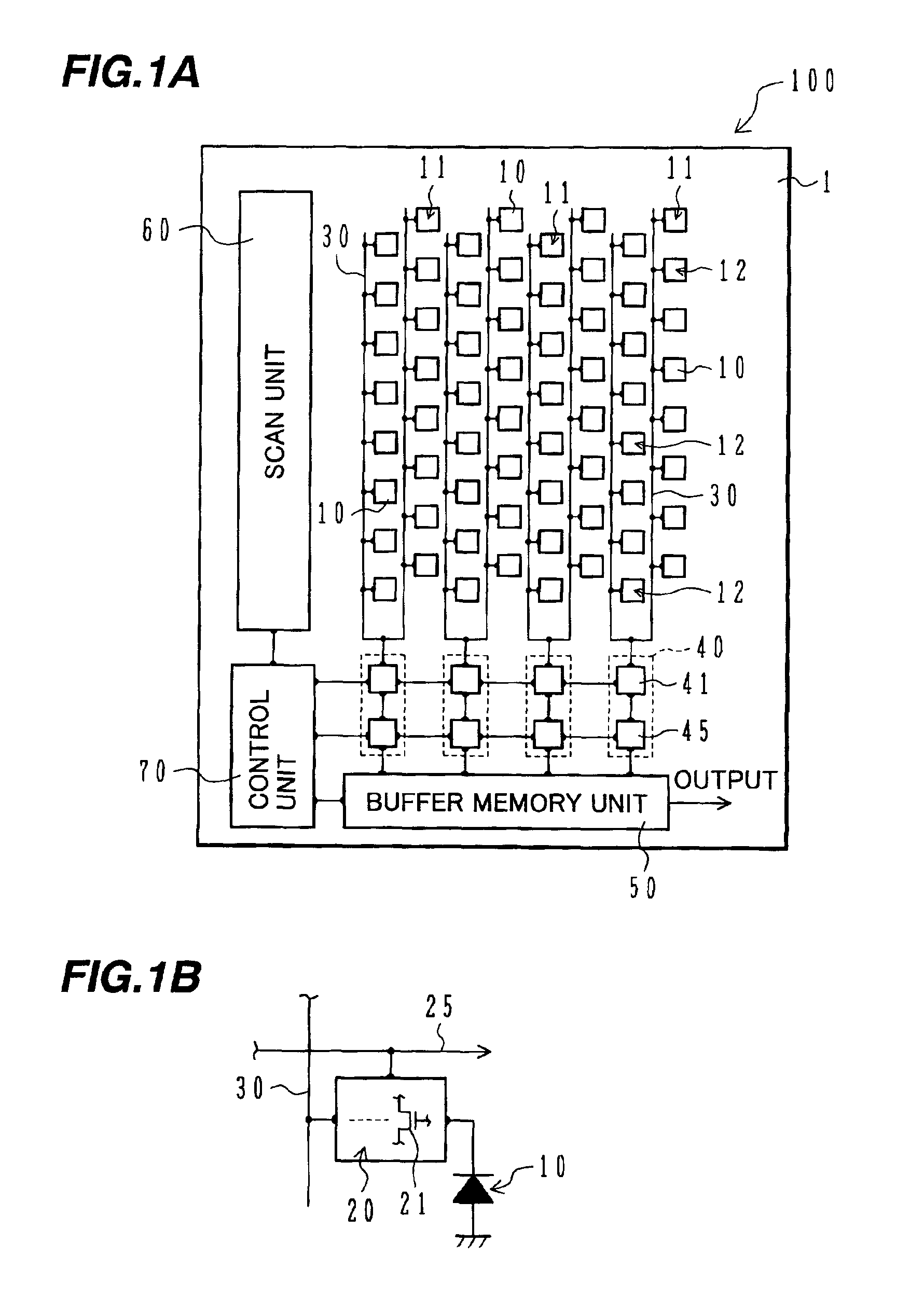
[0044]FIG. 1A is a schematic plan view of a MOS type solid-state image pickup device 100 according to the As shown, a number of photoelectric conversion elements or photodiodes 10 are disposed on the principal surface of a semiconductor substrate 1 in a pixel shift layout. In this simplified structure shown in FIG. 1A, the MOS type solid state image pickup device 100 has sixty four photoelectric conversion elements 10 disposed in the pixel shift layout of 16 rows and 8 columns. In an actual MOS type solid-state image pickup device, the total number of photoelectric conversion elements reaches, for example, several hundred thousands to several millions.

[0045]If the semiconductor substrate 1 is an n-type silicon substrate having p-type wells, each photoelectric conversion element 10 can be formed, for example, by forming an n-type region in the p-type well. By forming a p+-type region in the surface of the n-type region, a photoelectric conversion element 10 made of a buried type pho...

second embodiment

[0163]A MOS type solid-state image pickup device will be described with reference to FIGS. 9 and 10.

[0164]FIG. 9 is a schematic plan view of a MOS type solid-state image pickup device 200 of the second embodiment.

[0165]FIG. 10 is a diagram showing an example of the equivalent circuit of the switching circuit units 120a and the photoelectric conversion elements 10 constituting the MOS type solid-state image pickup device 200 shown in FIG. 9.

[0166]The MOS type solid state image pickup device 200 of the second embodiment is different from the MOS type solid state image pickup device 100 of the first embodiment in that (i) one output signal line 30 is disposed for each pair of adjacent photoelectric conversion element columns 11 with positioning therebetween as viewed in plan, (ii) one power supply voltage wiring line 31 is disposed for each pair of adjacent photoelectric conversion element columns 11 with positioning therebetween as viewed in plan, (iii) one A / D conversion unit 40 is ...

third embodiment

[0178]A MOS type solid-state image pickup device will be described with reference to FIG. 12.

[0179]FIG. 12 is a schematic cross sectional view of a MOS type solid-state image pickup device 210 according to the third embodiment. The MOS type solid state image pickup device 210 shown in FIG. 12 is a MOS type solid state color image pickup device having light shielding film 80, a color filter array 85, a micro lens array 90 and the like added to the MOS type solid state image pickup device 100 of the first embodiment.

[0180]The cross sectional view showing the semiconductor substrate 1, photoelectric conversion element 10, row select signal wiring line 25 and reset signal supply wiring line 32 shown in FIG. 12 is almost the same as a cross sectional view of the MOS type solid state image pickup device 100 taken along line A—A shown in FIG. 3.

[0181]As shown in FIG. 12, the MOS type solid-state image pickup device 210 has an n-type silicon semiconductor substrate 1 with p-type wells 1a f...


PUM


Abstract

A number of photoelectric conversion elements are disposed in a plurality of rows and columns in a pixel shift layout, and an analog / digital conversion unit is provided per two photoelectric conversion element columns to form a MOS type solid-state image pickup device. It is possible to suppress an increase in the manufacture cost of MOS type solid state image pickup devices with built-in A / D conversion units and improve the integration degree of photoelectric conversion elements.

Description

[0001]This application is based on Japanese Patent Application 2000-33929 filed on Feb. 10, 2000, the entire contents of which are incorporated herein by reference.BACKGROUND OF THE INVENTION[0002]a) Field of the Invention[0003]The present invention relates to a solid-state image pickup device, and more particularly to a solid-state image pickup device of a MOS (metal oxide semiconductor) type having analog / digital converters.[0004]b) Description of the Related Art[0005]After the establishment of mass production techniques for CCD (charge coupled device), apparatus utilizing CCD type solid-state image pickup devices as line (linear) sensors or area image sensors are rapidly prevailing.[0006]With the spread of portable remote terminals, MOS type solid state image pickup devices having a smaller power consumption than that of CCD type solid image pickup devices, particularly MOS type solid state image pickup devices with built-in analog / digital conversion units (hereinafter abbreviate...

Claims


Application Information

Patent Timeline
Patent Type & Authority Patents(United States)
IPC IPC(8): H04N9/04H04N3/15H01L27/14H01L27/146H01L31/10H04N5/335H04N5/349H04N5/369H04N5/374H04N5/378
CPCH04N3/1575H04N9/045H04N25/76H01L27/14
Inventor SUZUKI, NOBUOMASUKANE, KAZUYUKI
Owner FUJIFILM CORP
Why Eureka
Try Eureka