Substrate having a plurality of bumps, method of forming the same, and method of bonding substrate to another

a technology of substrates and bumps, which is applied in the direction of printed circuit manufacturing, printed circuit electric connection formation, printed circuit aspects, etc., can solve the problems of chip not being properly mounted on the circuit board, the bumps having the bumps b>60/b> cannot be formed uniformly by electrolytic plating methods, etc., and achieves the effect of easy positioning and accurate positioning

Inactive Publication Date: 2005-08-30
DENSO CORP
View PDF15 Cites 26 Cited by
  • Summary
  • Abstract
  • Description
  • Claims
  • Application Information

AI Technical Summary

Benefits of technology

[0015]In the above bonding method, the first substrate can be positioned easily and accurately to the second substrate when the first substrate is stacked on the second substrate, because the bump of the first substrate

Problems solved by technology

Therefore, the bump 60 cannot be formed uniformly by the electrolytic plating method.
Thus, it is difficult to mount the semiconductor chip having the bumps 60 o

Method used


Image

  • Substrate having a plurality of bumps, method of forming the same, and method of bonding substrate to another
  • Substrate having a plurality of bumps, method of forming the same, and method of bonding substrate to another
  • Substrate having a plurality of bumps, method of forming the same, and method of bonding substrate to another

Examples


first embodiment

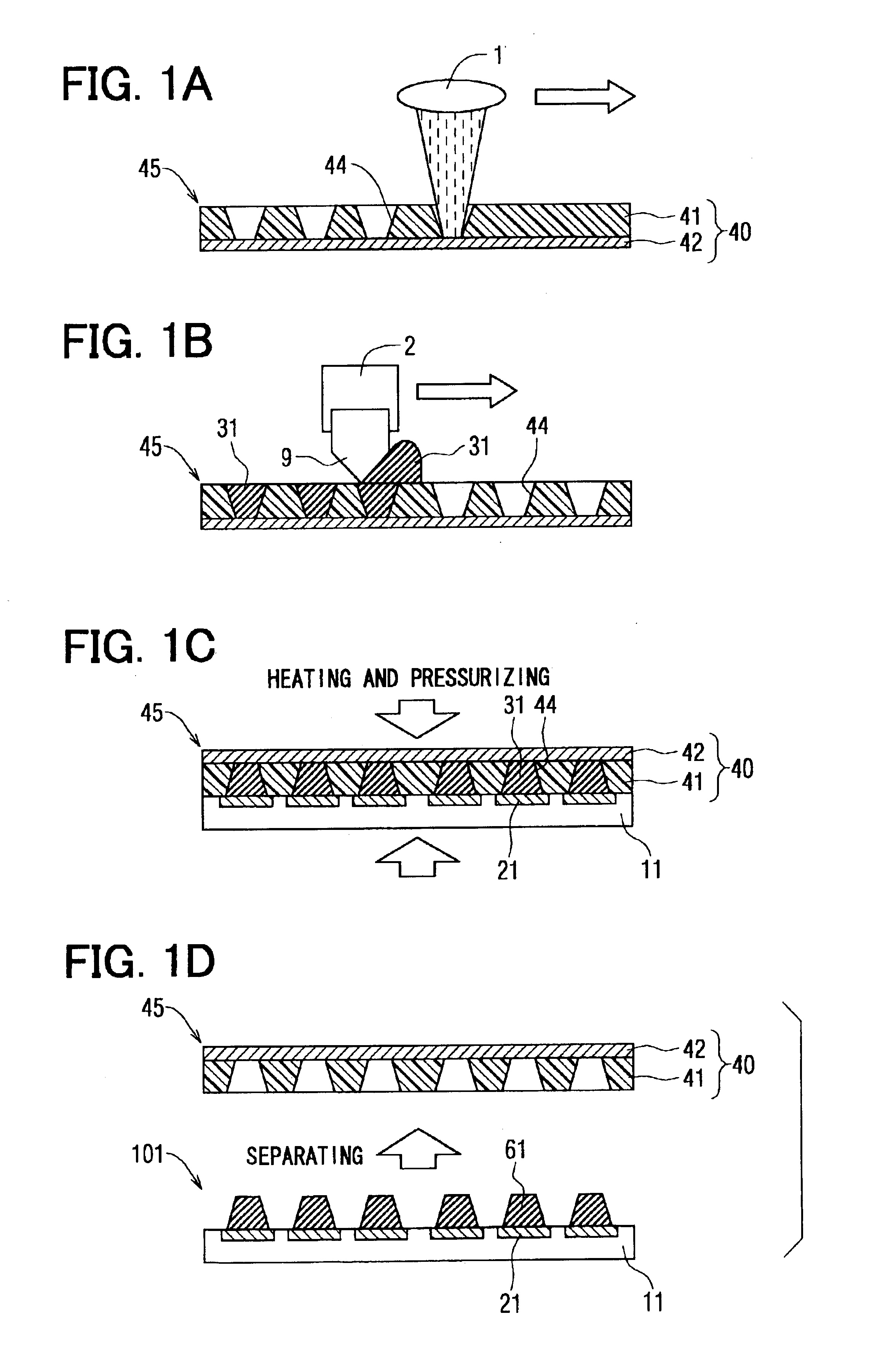
[0024](First Embodiment)

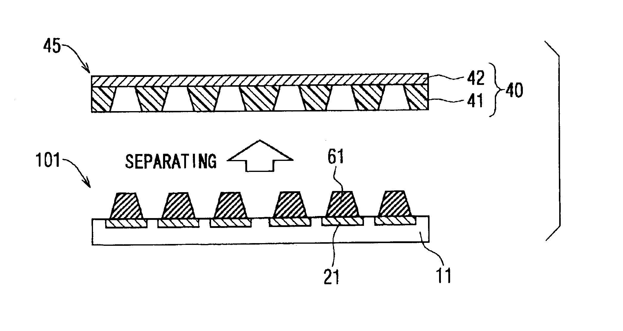
[0025]Referring first to FIG. 1A, a sheet 45 is prepared. The sheet 45 is composed of a bonded film 40, which includes a film 41 and a metallic film 42. The film 41 is bonded to the metallic film 42. Preferably, the film 41 is made of thermoplastic resin, for example, liquid crystal polymer, polyether ether ketone resin, polyether imide resin, and mixture of polyether ether ketone resin and polyether imide resin. These materials have moderate flexibility and heat resistance, so that a bump 61 shown in FIG. 1D can be easily formed.

[0026]More preferably, the coefficient of linear expansion of the film 41 is almost equal to that of a semiconductor substrate 11 shown in FIG. 1D, because the film 41 is disposed on the substrate 11 and then heated. Therefore, when a difference of the coefficient of linear expansion between the film 41 and the substrate 11 is comparatively large, filler is added in the film 41 so that the difference of the coefficient of the linear ...

second embodiment

[0057](Second Embodiment)

[0058]A method for forming a bump, according to a second embodiment of the present invention, is applied to a printed circuit board, as shown in FIGS. 4A to 4D. First, a bump 61 is formed on a triple layer printed circuit board 14, which is made of thermoplastic resin. Here, another multi-layer printed circuit board or a single layer printed circuit board can be used as the circuit board 14. The circuit board 14 includes an electrode 23. Considering a position of the electrode 23 on the circuit board 14, a hole 44 is formed at a certain position in a sheet 47.

[0059]The sheet 47 is composed of a bonded film 46, which includes a film 41, a metallic film 42, and a separation film 43. The separation film 43 is formed on the film 41, and the film 41 is formed on the metallic film 42. Here, the thickness of the separation film 43 is 50 μm. The film 41 is made of thermoplastic resin, and the separation film 43 is made of poly-imide resin. Preferably, the film 41 is...

third embodiment

[0065](Third Embodiment)

[0066]A bonding method for bonding a substrate having a bump to another substrate, according to a third embodiment of the present invention, is described with reference to FIGS. 5A to 5D.

[0067]At first, a semiconductor chip 12 having a bump 61 and a double layer printed circuit board 15 are prepared. The circuit board 15 has a plurality of holes 16 formed by the laser beam machine 1, and the hole 16 of the circuit board 15 corresponds to the bump 61 of the chip 12. The hole 16 has a bottom of an inner layer printed circuit 24. The hole 16 is filled with a metallic paste 32 with using a filling machine 2.

[0068]Next, as shown in FIG. 5C, the chip 12 having the bump 61 is reversed, and is stacked on the circuit board 15 so that the bump 61 of the chip 12 faces the hole 16 filled with the metallic paste 32. Then, the circuit board 15 with the chip 12 is heated and pressurized with using a hot-press machine (not shown).

[0069]Thus, the metallic paste 32 is sintered...


PUM

PropertyMeasurementUnit
Temperatureaaaaaaaaaa
Thicknessaaaaaaaaaa

Abstract

A plurality of bumps is formed on a substrate. At first, a hole having a bottom is formed in a sheet, and the hole is filled with a metallic paste. Then, the sheet is stacked and positioned on the substrate so that the hole of the sheet faces an electrode of the substrate. The substrate with the sheet is heated and pressurized so that the metallic paste is sintered and bonded to the electrode so as to form the bump. Then, the sheet is separated from the substrate having the bump, so that the bump is formed on the substrate. A part of each bump does not lack, and all of the bumps are formed surely. Therefore, the bump can be formed uniformly.

Description

CROSS REFERENCE TO RELATED APPLICATION[0001]This application is based on Japanese Patent Application No. 2002-161735 filed on Jun. 3, 2002, the disclosure of which is incorporated herein by reference.FIELD OF THE INVENTION[0002]The present invention relates to a substrate having a plurality of bumps, method of forming a plurality of bumps of a substrate, and method of bonding a substrate having a plurality of bumps to another substrate.BACKGROUND OF THE INVENTION[0003]An electrolytic plating method is well known as a method for forming a bump on an electrode of a semiconductor substrate. This electrolytic plating method according to a related art is described as follows.[0004]As shown in FIG. 7, a semiconductor substrate 11, which is made of silicon wafer, includes a plurality of electrodes 21. A photo-resist mask 70 is formed on the substrate 11, and has an opening for forming a bump 60 on a surface of the electrode 21. The substrate 11 is dipped in plating solution 4.[0005]The ele...

Claims


Application Information

Patent Timeline
IPC IPC(8): H01L21/67H01L21/48H01L21/02H01L23/48H01L21/68H01L23/498H05K3/40H05K3/46H01L25/065H05K3/20H05K3/00H05K1/09H01L21/60
CPCH01L21/4853H01L21/6835H01L23/481H01L23/49811H05K3/4007H05K3/4617H01L21/4867H01L2224/16235H01L25/0657H01L2224/11003H01L2224/11505H01L2224/16H01L2924/01078H01L2924/01079H05K1/095H05K3/0035H05K3/207H05K2201/0367H05K2201/0394H05K2203/0113H05K2203/0338H01L2224/1111H01L2224/05571H01L2224/05573H01L2224/05647H01L21/76898H01L24/05H01L2924/00014
Inventor SAKAIDA, ATUSI
Owner DENSO CORP
Why Eureka
Try Eureka