Heterojunction bipolar transistor with a base layer that contains bismuth

a bipolar transistor and base layer technology, applied in the field of semiconductor devices, can solve the problems of reducing the maximum oscillation frequency fsub>max, the reduction of the base resistance is an important challenge, and the non-adjustable operation of the electromechanical device, so as to improve the basic performance of the hbt, reduce the base resistance, and improve the moving speed of the electrons

Inactive Publication Date: 2005-08-30
SONY CORP
View PDF4 Cites 17 Cited by
  • Summary
  • Abstract
  • Description
  • Claims
  • Application Information

AI Technical Summary

Benefits of technology

[0019]The present invention has been made in view of the above-recited problems to be solved to provide higher efficiency when an HBT is used as a device for a PA and to provide improved basic performance of the HBT, such as reduced base resistance. There is a need to provide a semiconductor device that achieves improved PA characteristics over the conventional PA using GaAs-based HBT or InP-based HBT.

Problems solved by technology

However, the graded heterojunction is not necessarily made easily with favorable controllability and reproducibility, and a thick graded layer is needed to eliminate the influence of the conduction-band offset ΔEc and so that holes are not confined completely within the base layer, so that it is desirable to reduce the offset voltage Voffset by lowering the offset voltage ΔEc.
From the viewpoint of improvement in basic performance of the HBT, a reduction in base resistance is an important challenge.
When the base resistance is high, some disadvantages occur such as a reduction in the maximum oscillation frequency fmax and uneven voltage applied between the emitter and the base (emitter crowding) in areas where the current density is high.
The doping concentration, however, cannot be increased without limitation since the doping concentration has an upper limit and an extremely high doping concentration causes problems such as a reduced current gain and reduced carrier mobility.

Method used


Image

  • Heterojunction bipolar transistor with a base layer that contains bismuth
  • Heterojunction bipolar transistor with a base layer that contains bismuth
  • Heterojunction bipolar transistor with a base layer that contains bismuth

Examples


first embodiment

(First Embodiment)

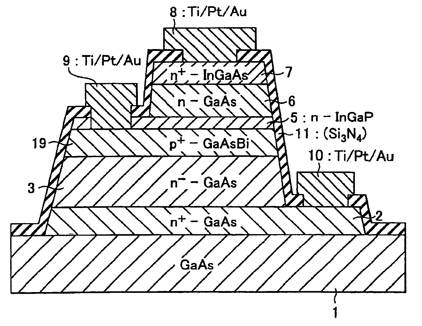
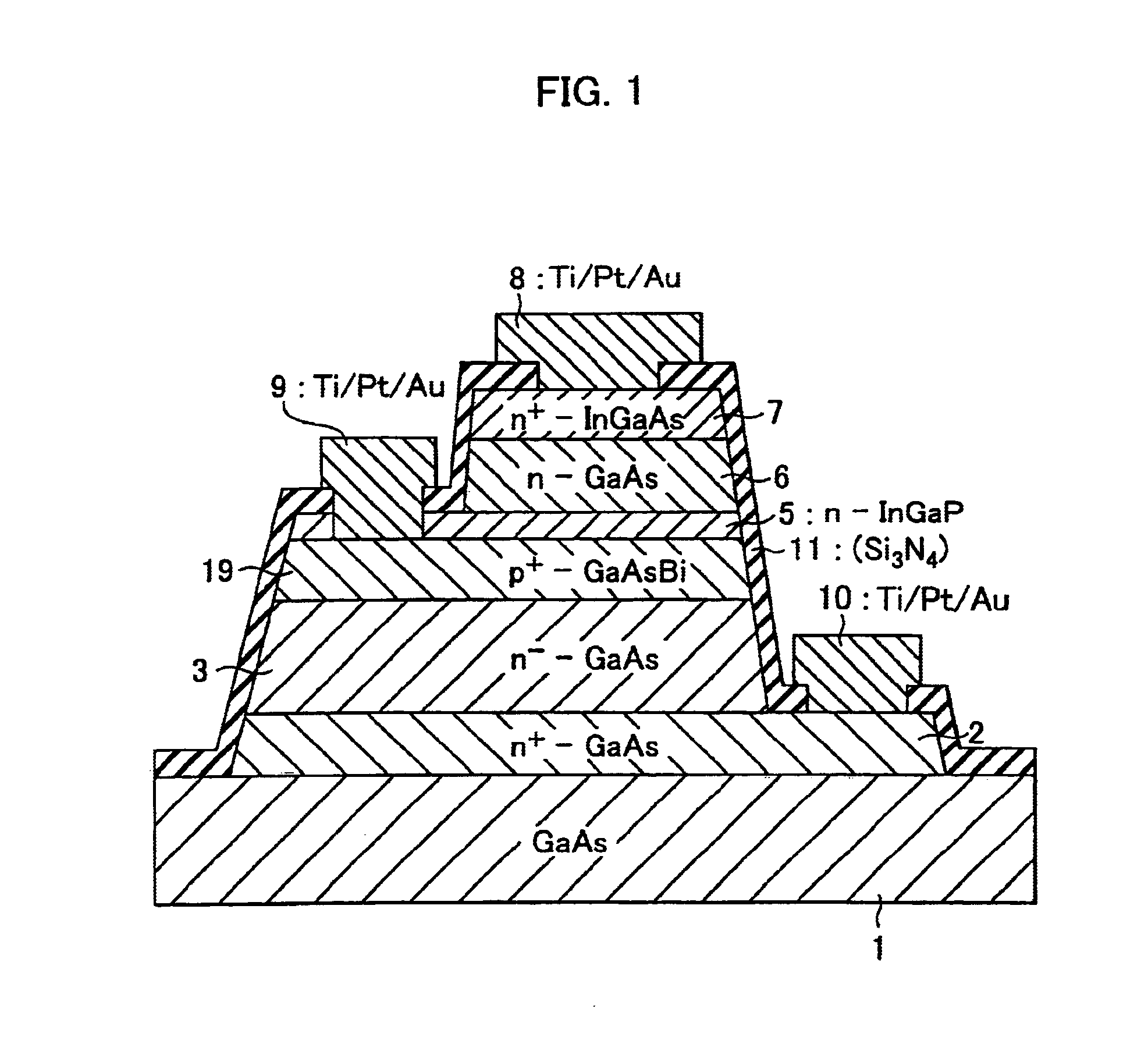
[0038]FIG. 1 shows a semiconductor device according to a first embodiment of the present invention. GaAsBi is used for a base layer, and the remaining configuration is the same as the configuration shown in FIG. 7. In FIG. 1, components identical to those in FIG. 7 are designated with the same reference numerals.

[0039]As shown in FIG. 1, the semiconductor device according to the first embodiment includes a subcollector layer 2, made of, for example, n+-GaAs, a collector layer 3 made of n−-GaAs, a base layer 19 made of p+-GaAsBi, an emitter layer 5, made of, for example, n-InGaP, a first cap layer 6 made of n-GaAs, and a second cap layer 7 made of n+-InGaAs, which are successively stacked on a substrate 1, made of, for example, semi-insulating single crystal GaAs.

[0040]An emitter electrode 8 is formed on the second cap layer 7. For forming a base contact, portions of the first and second cap layers are removed to form a mesa structure. The emitter layer 5 may be int...

second embodiment

(Second Embodiment)

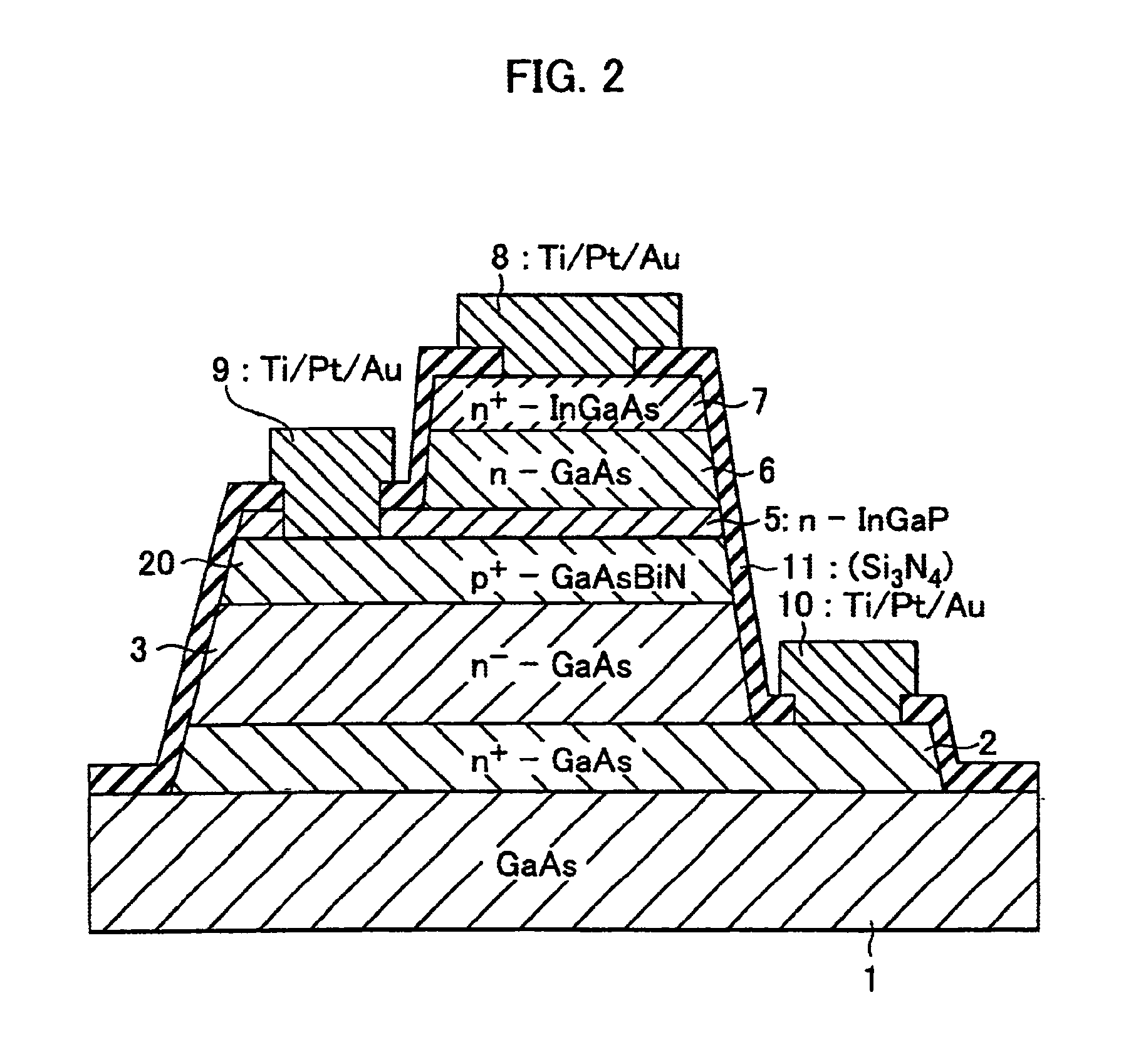
[0043]FIG. 2 shows a semiconductor device according to a second embodiment of the present invention, in which GaAsBiN is used for a base layer. Specifically, the second embodiment differs from the first embodiment shown in FIG. 1 in that the base layer 19 made of p+-GaAsBi is replaced with a base layer 20 made of p+-GaAsBiN, and the remaining portions are the same as in the first embodiment.

[0044]In this configuration, the addition of Bi to GaAs serves to make the lattice constant of the crystal larger than GaAs, although the addition of N (nitrogen) serves to make the lattice constant smaller. This reduces the lattice mismatch between the base layer and the GaAs layer (the collector layer) found in the first embodiment. Thus, it is possible to form a thicker base layer than the base layer made of GaAsBi or to increase the energy level at the valence band edge by increasing the amount of Bi, while the advantages described in the first embodiment are maintained. Co...

third embodiment

(Third Embodiment)

[0046]FIG. 3 shows a semiconductor device according to a third embodiment of the present invention, in which GaAsBiN is used for a base layer, and GaAs is used for an emitter layer. Specifically, the third embodiment differs from the second embodiment in that an emitter layer 21 made of n-GaAs and a cap layer 22 made of n+-InGaAs are successively stacked on the base layer 20 made of p+-GaAsBiN. The remaining portions are the same as in the first and second embodiments.

[0047]In the above configuration, as compared with the emitter layer made of InGaP used in the first and second embodiments, the energy at the conduction band edge of the emitter is reduced to lower the turn-on voltage at the emitter-base junction. Thus, the Knee voltage Vk in the Ic−Vce characteristics can be reduced. The reduction in the Knee voltage Vk is important since it increases the power added efficiency (PAE) of a power amplifier (PA). The emitter layer made of GaAs is effective because GaAs...


PUM


Abstract

A heterojunction bipolar transistor (HBT) with improved characteristics is provided. A III-V compound semiconductor having Bi added thereto is used for a base layer of a GaAs-based or InP-based HBT. For example, a GaAs-based HBT is formed by successively stacking a subcollector layer made of n+-GaAs, a collector layer made of n−-GaAs, a base layer made of p+-GaAsBi, an emitter layer made of n-InGaP, a first cap layer made of n-GaAs, and a second cap layer made of n+-InGaAs on a substrate 1 made of single crystal GaAs.

Description

CROSS REFERENCE TO RELATED APPLICATION[0001]This application claims priority from Japanese Priority Document No. 2002-225631, filed on Aug. 2, 2002 with the Japanese Patent Office, which document is hereby incorporated by reference.BACKGROUND OF THE INVENTION[0002]1. FIELD OF THE INVENTION[0003]The present invention relates generally to a semiconductor device, and more particularly, to a heterojunction bipolar transistor.[0004]2. DESCRIPTION OF RELATED ART[0005]A heterojunction bipolar transistor (hereinafter referred to as a HBT) is a kind of bipolar transistor having an emitter layer made of a material with a wider band gap than a material of a base layer, in which high injection efficiency (emitter injection efficiency) of electrons from the emitter layer to the base layer can be assured even when the base layer has an impurity concentration higher than the emitter layer. Thus, the base layer can have low resistance even with a reduced thickness, and a punch-through phenomenon ac...

Claims


Application Information

Patent Timeline
Patent Type & Authority Patents(United States)
IPC IPC(8): H01L21/331H01L21/02H01L29/737H01L31/06H01L31/072H01L31/0264H01L31/0328H01L31/0336H01L29/66H01L29/10H01L29/201H01L29/205H01L29/70H01L31/109
CPCH01L29/0817H01L29/0821H01L29/1004H01L29/7371H01L29/205H01L29/66318H01L29/201H01L29/737
Inventor HASE, ICHIRO
Owner SONY CORP
Why Eureka
Try Eureka