Nonvolatile silicon/oxide/nitride/silicon/nitride/oxide/silicon memory

a technology of silicon/oxide/nitride/silicon and nonvolatile memory, which is applied in the direction of solid-state devices, instruments, semiconductor devices, etc., to achieve the effect of improving the programming rate and the memory capacity

Active Publication Date: 2005-08-30
SAMSUNG ELECTRONICS CO LTD
View PDF1 Cites 71 Cited by
  • Summary
  • Abstract
  • Description
  • Claims
  • Application Information

AI Technical Summary

Benefits of technology

[0012]The present invention provides a memory device having a high programming operation rate and a high storage capacity using the advantages of a silicon / oxide / nitride / silicon / nitride / oxide / silicon (SONSNOS) memory structure.
[0024]The SONSNOS memory according to the present invention increases the number of trap sites for storing the electrons to improve the programming rate and the capacity of the memory.

Problems solved by technology

However, since a flash memory has a disadvantages of low retention, a silicon / oxide / nitride / oxide / silicon (SONOS) memory device may only be used for increasing information storage capacity and improving process performance.

Method used


Image

  • Nonvolatile silicon/oxide/nitride/silicon/nitride/oxide/silicon memory
  • Nonvolatile silicon/oxide/nitride/silicon/nitride/oxide/silicon memory
  • Nonvolatile silicon/oxide/nitride/silicon/nitride/oxide/silicon memory

Examples


first embodiment

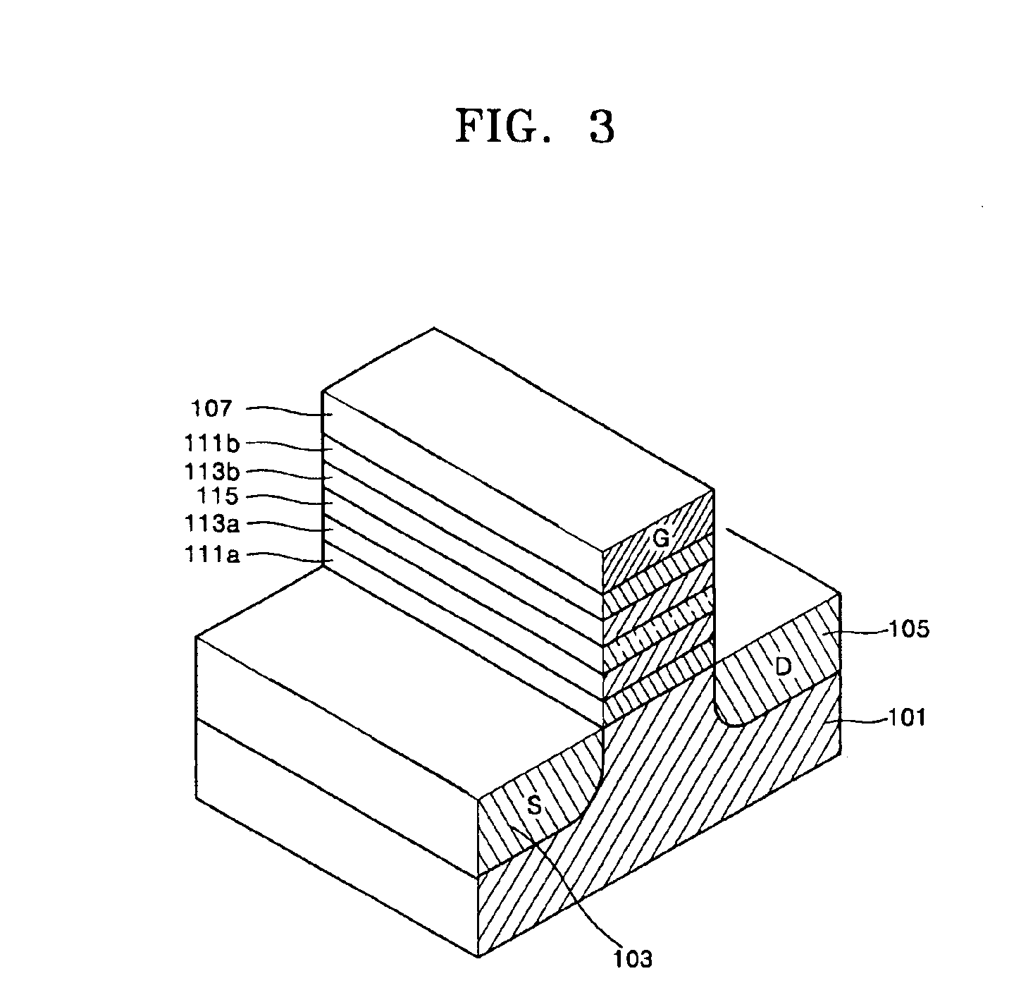
[0036]FIG. 3 illustrates a perspective view of silicon / oxide / nitride / silicon / nitride / oxide / silicon (SONSNOS) memory according to the present invention.

[0037]Referring to FIG. 3, a gate electrode 107 is located on a substrate 101 having a source electrode 103 and a drain electrode 105, and a multi-layered ONSNO layer is interposed between the substrate 101 and the gate electrode 107 to trap electrons. An electron channel is formed between the source and drain electrodes 103 and 105. Here, the gate electrode 107 may be formed using a semiconductor, such as silicon (Si), or a metal.

[0038]The ONSNO layer includes first and second oxide layers 111a and 111b, respectively, located on the substrate 101 and under the gate electrode 107; first and second nitride layers 113a and 113b, respectively, located on the first oxide layer 111a and under the second oxide layer 111b; and a silicon layer 115 interposed between the first and second nitride layers 113a and 113b.

[0039]The first and second...

second embodiment

[0044]FIG. 4A illustrates a perspective view of an SONSNOS memory cell according to the present invention.

[0045]Reference numeral 121 denotes a substrate, 123 denotes a source electrode, 125 denotes a drain electrode, 127 denotes a gate electrode, 131a denotes a first oxide layer, 131b denotes a second oxide layer, 133a denotes a first nitride layer, 133b denotes a second nitride layer, and 135 denotes silicon quantum dots. The structure of the SONSNOS memory cell according to the second embodiment of the present invention is similar to the structure of the SONSNOS memory cell according to the first embodiment of the present invention, except for the inclusion of the silicon quantum dots 135 in the place of the silicon layer (115 of FIG. 3). Alternately, metal quantum dots may be formed of gold (Au) or aluminum (Al) instead of the silicon quantum dots 135.

[0046]FIG. 4B illustrates an enlarged view of a circular portion ‘A’ of FIG. 4A.

[0047]The silicon quantum dots 135 can be substit...

third embodiment

[0052]FIG. 5 illustrates a sectional view of a multi-layered SONSNOS memory cell according to the present invention.

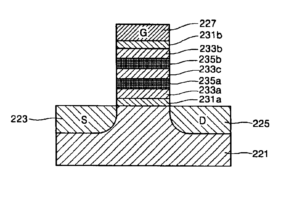
[0053]Referring to FIG. 5, an oxide / nitride / silicon / nitride / silicon / nitride / oxide (ONSNSNO) layer is interposed between a substrate 201 and a gate electrode 207. A source electrode 203 and a drain electrode 205 are formed in the substrate 201. The ONSNSNO layer includes first and second oxide layers 211a and 211b, located on the substrate 201 and under the gate electrode 207, respectively; first and second nitride layers 213a and 213b, arranged on the first oxide layer 211a and under the second oxide layer 211b, respectively; first and second silicon layers 215a and 215b, formed on the first nitride layer 213a and under the second nitride layer 213b, respectively; and a third nitride layer 213c interposed between the first and second silicon layers 215a and 215b.


PUM


Abstract

A nonvolatile silicon / oxide / nitride / silicon / nitride / oxide / silicon (SONSNOS) structure memory device includes a first insulating layer and a second insulating layer stacked on a channel of a substrate, a first dielectric layer and a second dielectric layer formed on the first insulating layer and under the second insulating layer, respectively, and a group IV semiconductor layer, silicon quantum dots, or metal quantum dots interposed between the first dielectric layer and the second dielectric layer. The provided SONSNOS structure memory device improves a programming rate and the capacity of the memory.

Description

BACKGROUND OF THE INVENTION[0001]1. Field of the Invention[0002]The present invention relates to a nonvolatile memory. More particularly, the present invention is directed to a silicon / oxide / nitride / silicon / nitride / oxide / silicon (SONSNOS) memory having an improved storage capacity.[0003]2. Description of the Related Art[0004]FIG. 1 illustrates a sectional view of a conventional flash electrically erasable programmable read only memory (EEPROM) cell. The flash EEPROM, as nonvolatile memory, stores data even in a power off state.[0005]Referring to FIG. 1, a gate electrode 17 is located on a substrate 11 having a source electrode 13 and a drain electrode 15. A gate oxide 21, a floating gate 23, and an insulating layer 25 are sequentially stacked between the gate electrode 17 and the substrate 11.[0006]In general, a flash memory is programmed using hot carriers that are injected from a portion of the substrate 11, in particular, the channel of electrons that is formed between the source...

Claims


Application Information

Patent Timeline
Patent Type & Authority Patents(United States)
IPC IPC(8): H01L21/28H01L21/02H01L29/423H01L29/51H01L29/788H01L29/66H01L29/40G11C16/04H01L21/8247H01L27/115H01L29/792
CPCB82Y10/00H01L21/28194H01L21/28273H01L21/28282H01L29/42332H01L29/513H01L29/7885H01L29/7887H01L29/7888G11C16/0475G11C2216/06H01L29/517H01L29/518H01L29/40114H01L29/40117H10B99/00
Inventor CHAE, SOO-DOOKIM, JU-HYUNGKIM, CHUNG-WOOCHAE, HEE-SOONRYU, WON-IL
Owner SAMSUNG ELECTRONICS CO LTD
Why Eureka
Try Eureka