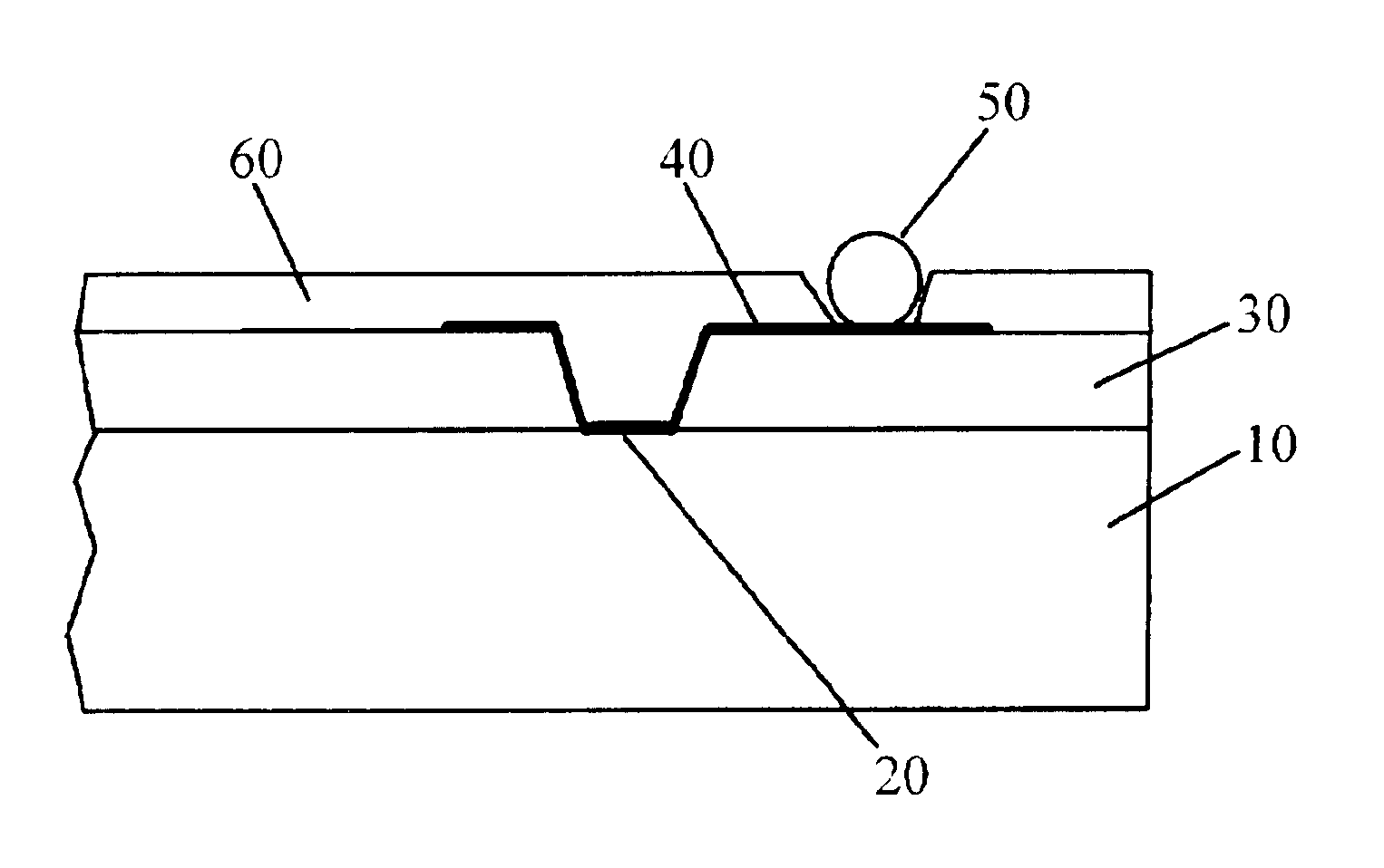
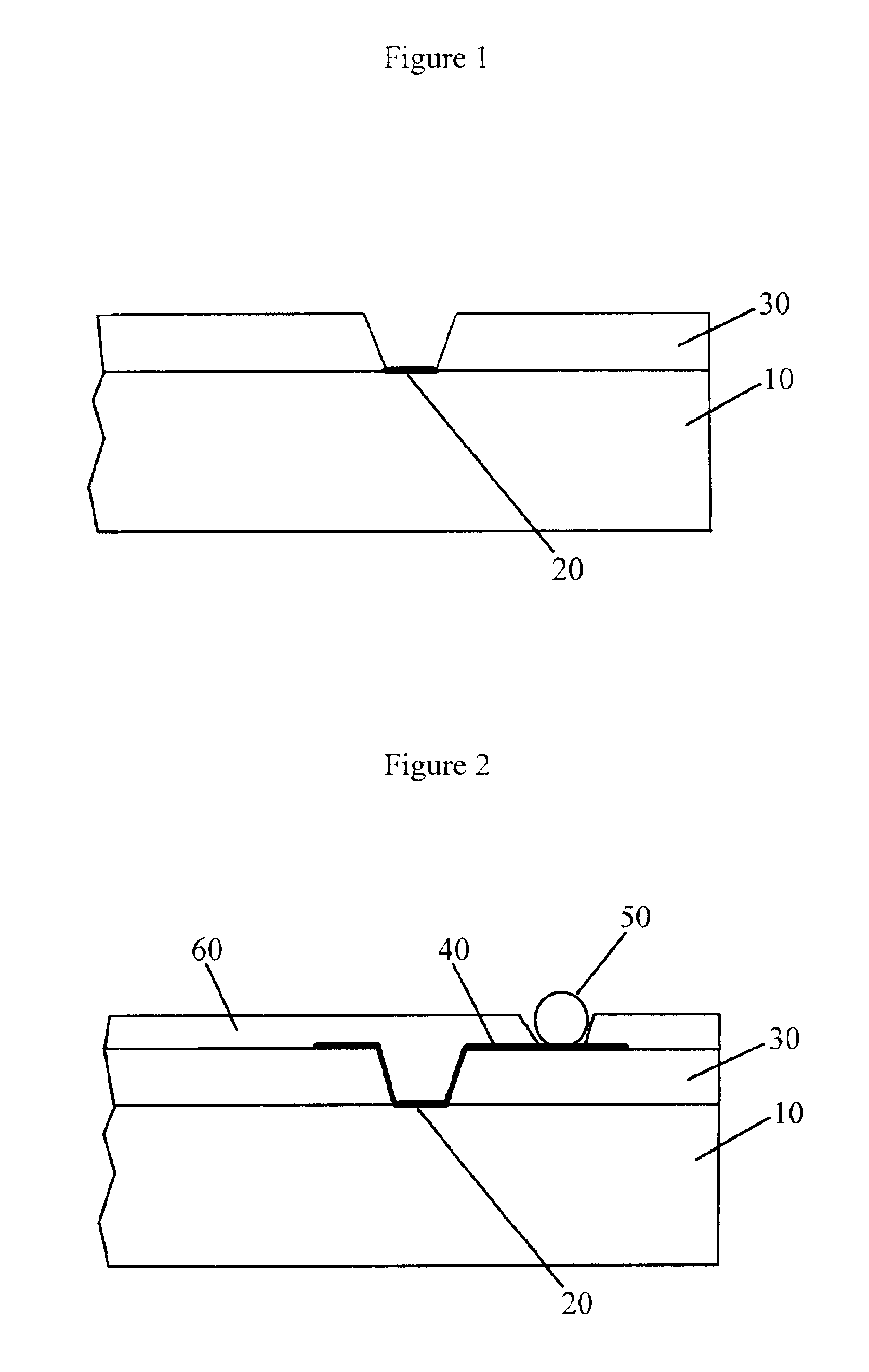
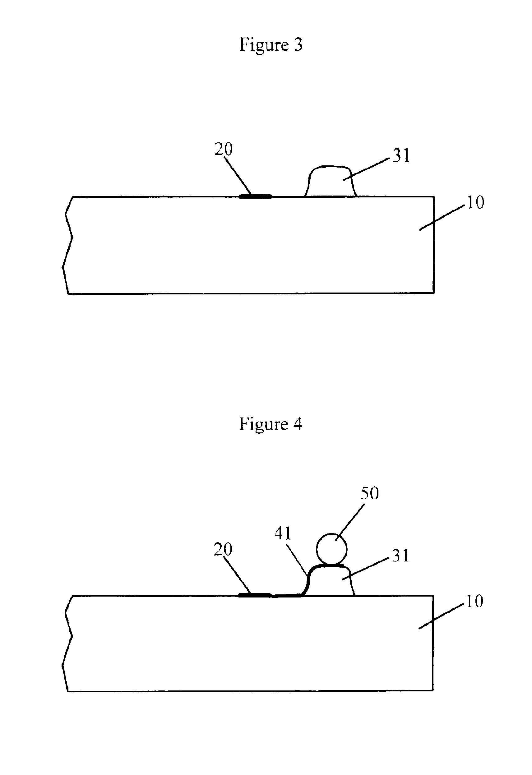
Semiconductor package and method of preparing same
a technology of semiconductor and ic package, which is applied in the field of semiconductor package, can solve the problems of limited reliability of ic package, and achieve the effects of good environmental resistance, good thermal stability, and high throughpu
- Summary
- Abstract
- Description
- Claims
- Application Information
AI Technical Summary
Benefits of technology
Problems solved by technology
Method used
Image

Examples
example 1
[0138]Polymer B (20.9 parts), 79.1 parts of Polymer D, 1.2 parts of Crosslinking Agent C, and 194.5 parts of Filler A were blended in a changed can mixer until the filler became uniformly distributed in the mixture. Inhibitor (0.04 part) and 3.7 parts of Catalyst were added to the mixture and mixing was continued for about 20 min. The silicone composition had a viscosity of 235.6 Pa·s at 1.0 rad / s and 193.4 Pa·s at 10 rad / s. The physical properties of the cured silicone product are shown in Table 1.
example 2
[0139]Polymer A (75.0 parts), 25.0 parts of Polymer B, 2.5 parts of Crosslinking Agent A, 3.2 parts of Crosslinking Agent B, 291.6 parts of Filler A, and 4.2 parts of Filler B were blended in a changed can mixer until the filler became uniformly distributed in the mixture. Inhibitor (0.05 part) and 2.5 parts of Catalyst were added to the mixture and mixing was continued for about 20 min. The silicone composition had a viscosity of 177.0 Pa·s at 1.0 rad / s and 27.9 Pa·s at 10 rad / s. The physical properties of the cured silicone product are shown in Table 1.
example 3
[0140]Polymer B (50.0 parts), 50.0 parts of Polymer C, 18.3 parts of Crosslinking Agent C, 345.3 parts of Filler A, and 9.8 parts of Filler B were blended in a changed can mixer until the filler became uniformly distributed in the mixture. Inhibitor (0.06 part) and 3.1 parts of Catalyst were added to the mixture and mixing was continued for about 20 min. The silicone composition had a viscosity of 322.8 Pa·s at 1.0 rad / s and 42.6 Pa·s at 10 rad / s. The physical properties of the cured silicone product are shown in Table 1.
[0141]
TABLE 1DurometerTensileChordHardnessStrengthElongationModulusCTEExample(Shore A)(MPa)(%)(MPa)(μm / m / ° C.)167.63.5199.903.5157293.06.4011.9153.8110392.06.284.23148.570
PUM
| Property | Measurement | Unit |
|---|---|---|
| thickness | aaaaa | aaaaa |
| mole ratio | aaaaa | aaaaa |
| mole ratio | aaaaa | aaaaa |
Abstract
Description
Claims
Application Information
 - R&D
- Intellectual Property
- Life Sciences
- Materials
- Tech Scout
- Unparalleled Data Quality
- Higher Quality Content
- 60% Fewer Hallucinations
Browse by: Latest US Patents, China's latest patents, Technical Efficacy Thesaurus, Application Domain, Technology Topic, Popular Technical Reports.
© 2025 PatSnap. All rights reserved.Legal|Privacy policy|Modern Slavery Act Transparency Statement|Sitemap|About US| Contact US: help@patsnap.com