Compound filled in lead IC packaging product

a technology of lead ic packaging and compound, which is applied in the direction of electrical equipment, semiconductor devices, semiconductor/solid-state device details, etc., can solve the problems of low manufacturing efficiency, contamination of contacts on the bottom of the lead frame, and troublesome qfn production lines. , to achieve the effect of low manufacturing tim

Inactive Publication Date: 2005-09-06
MUTUAL TEK INDS
View PDF5 Cites 8 Cited by
  • Summary
  • Abstract
  • Description
  • Claims
  • Application Information

AI Technical Summary

Benefits of technology

[0010]The primary objective of the present invention is to provide an improved encapsulated IC product with a molding compound or encapsulat

Problems solved by technology

The two processes prolong the entire manufacture process and thus the manufacture efficiency is low.
Although the QFN (Quad Flat Non-Leaded) product amount has increased in popularity in recent years, the same problem bothers the QFN production line.
However, the molding compound or encapsulation material may flow to the bottom of the lead frame and the contacts on the bottom of the lead frame are contaminated.
Although either method effectively stops encapsul

Method used


Image

  • Compound filled in lead IC packaging product
  • Compound filled in lead IC packaging product
  • Compound filled in lead IC packaging product

Examples


Embodiment Construction

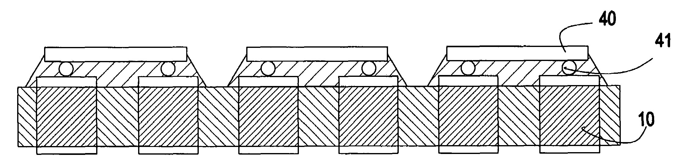
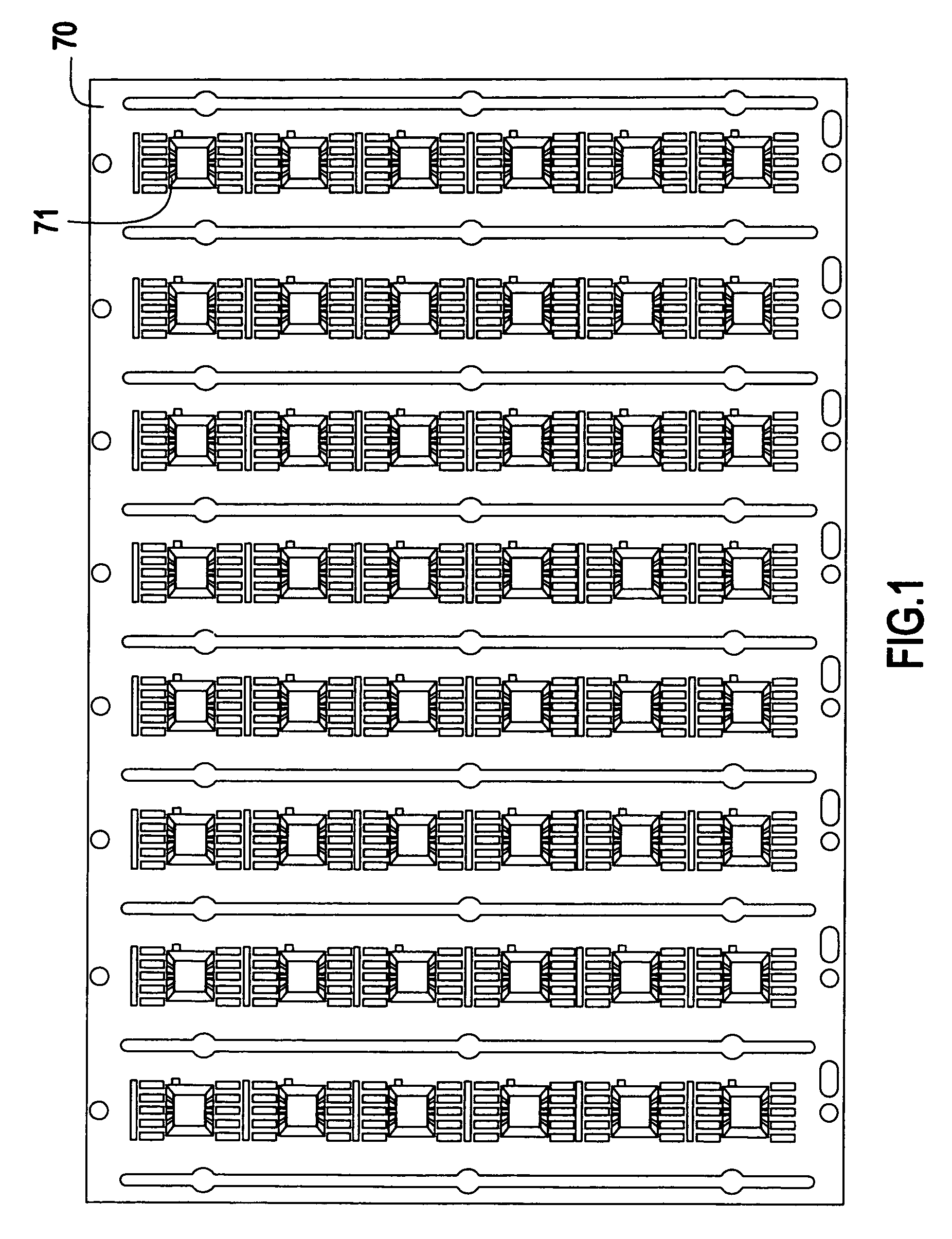
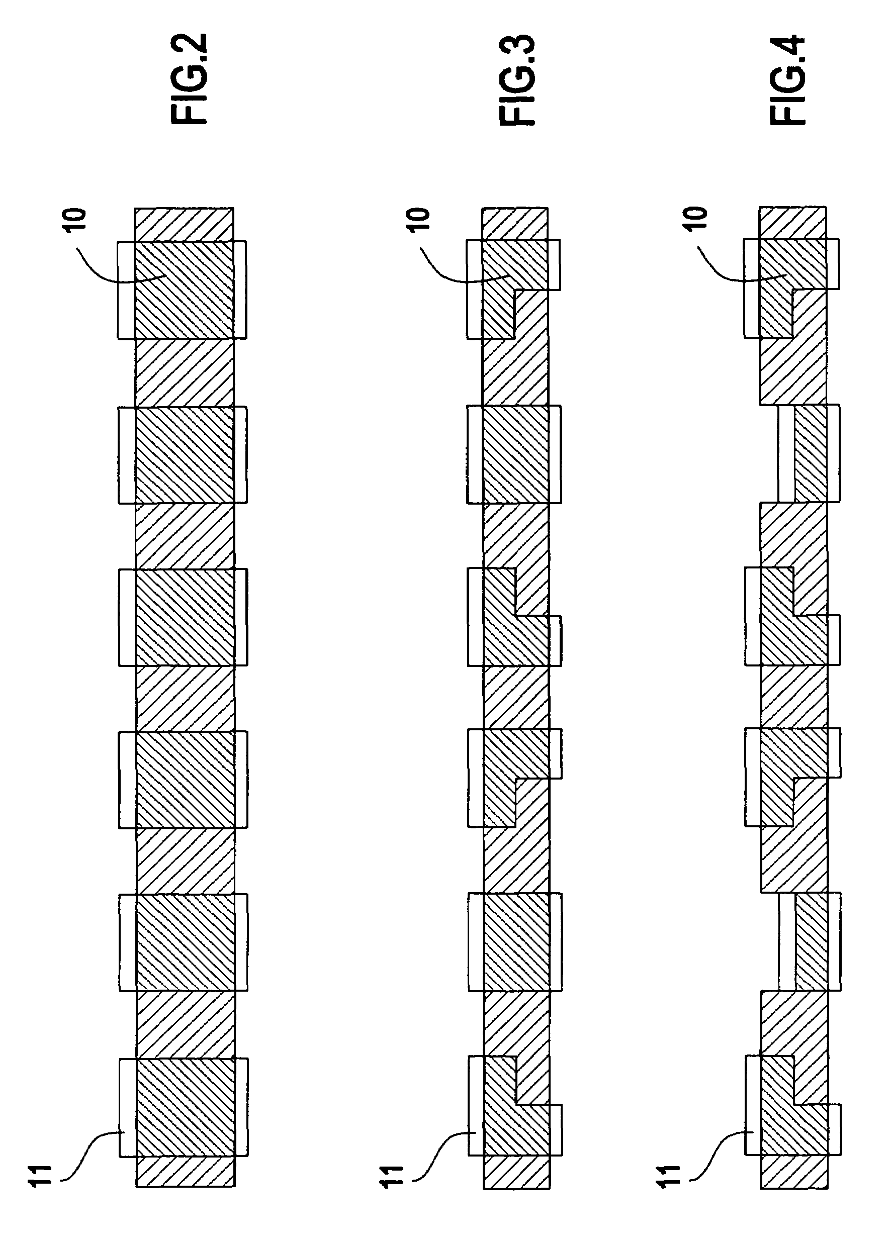
[0022]With reference to FIGS. 2–4, the compound filled in lead packaging IC product of the present invention includes a solid substrate (10) with a surrounding compound or encapsulation material in support of the substrate (10). A metallic protection layer (11), i.e. gold, nickel, silver, cobalt or a combination thereof, is plated onto the surfaces of the substrate (10) to allow electrical communication between a top face and a bottom face of the substrate (10) and to protect the wire (12) or to provide an adhesive function for electrical appliance attachment. The substrate (10) made of metal may be of any desired shape to adapt to electricity and thermal characteristics of the designed product. A plating process and an etching process may be involved in the preparation of the substrate (10). The encapsulation material (20) functions are to ① support the substrate; ② function as a dielectric material; ③ function as a heat conductor; ④ function as a stop to prevent encapsulation mate...


PUM


Abstract

A compound filled in lead packaging integrated circuit product includes a substrate made of a metallic material, a metallic protection layer formed on a top face of the substrate for protection of the substrate and surface mounting of an electrical appliance, the electrical appliance securely mounted on the protection layer and a compound or encapsulation material surrounding the substrate and the electrical appliance for supporting the substrate.

Description

BACKGROUND OF THE INVENTION[0001]1. Field of the Invention[0002]The present invention relates to a compound filled in lead integrated circuit package product, and more particularly to a substrate made of metal and filled in with compound or encapsulation material to support the lead of the packaged IC product.[0003]2. Description of Related Art[0004]In a conventional encapsulated integrated circuit (IC) product, the lead frame (70) is hollow and the lead (71) on top of the lead frame (70) is a continuous wire, as shown in FIG. 1. The lead (71) has to be continuous so as to support each other in the manufacture process. The lead frame (70) has to undergo a trimming process and a forming process to cut off and bend the lead (71) to avoid interference between each semi-product. The two processes prolong the entire manufacture process and thus the manufacture efficiency is low. Although the QFN (Quad Flat Non-Leaded) product amount has increased in popularity in recent years, the same p...

Claims


Application Information

Patent Timeline
IPC IPC(8): H01L23/28H01L21/56H01L23/31H01L23/498
CPCH01L23/3121H01L23/49827H01L24/97H01L21/563H01L23/49861H01L2224/16245H01L2224/48091H01L2224/48247H01L2224/73265H01L2224/97H01L2924/01027H01L2924/01047H01L2924/01078H01L2924/01079H01L2924/01082H01L2924/14H01L2224/85H01L2924/00014H01L2224/81H01L2224/83H01L24/48H01L2224/73204H01L2924/181H01L2224/45144H01L24/45H01L2924/00012H01L2224/45015H01L2924/207
Inventor HWAN, LU-CHEN
Owner MUTUAL TEK INDS
Why Eureka
Try Eureka