Analog optical black clamping circuit for a charge coupled device having wide programmable gain range
Active Publication Date: 2005-09-06
TEXAS INSTR INC
View PDF13 Cites 28 Cited by
Summary
Abstract
Description
Claims
Application Information
AI Technical Summary
This helps you quickly interpret patents by identifying the three key elements:
Problems solved by technology
Method used
Benefits of technology
[0008]The image processing apparatus may be implemented using switch capacitors. In addition, this design provides further flexibility in that the programmable gain amplifiers and the reverse programmable gain amplifier may be implemented using single-ended or differential amplifiers.
[0009]Advantages of this design include but are not limited
Problems solved by technology
In addition, this approach relies on devic
Method used
Image
Click on the blue label to locate the original text in one second.
Reading with bidirectional positioning of images and text.
Examples
Embodiment Construction
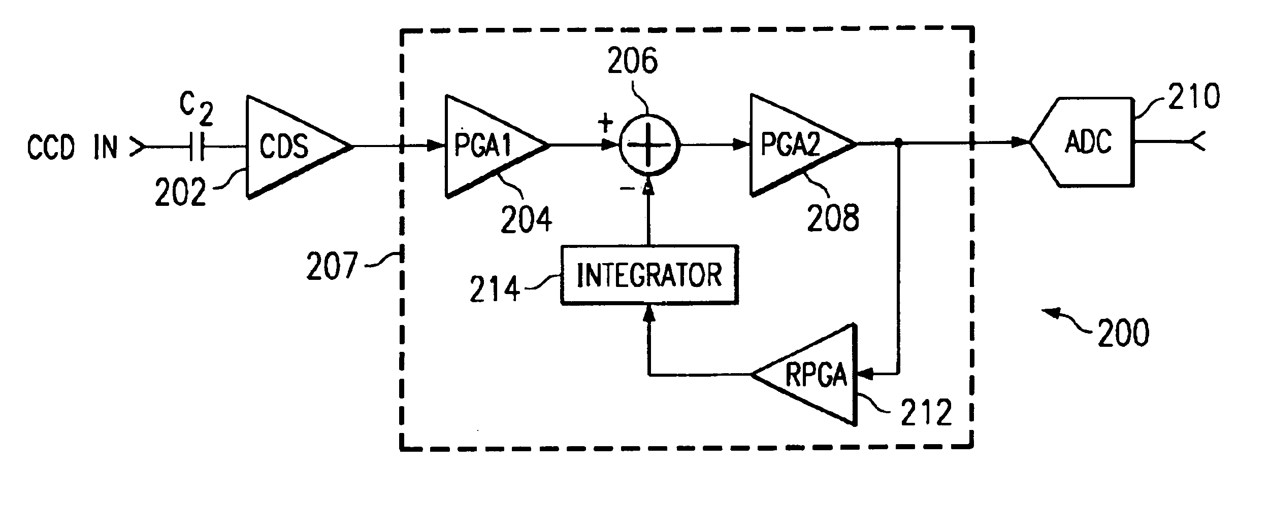
[0014]In accordance with the present invention, the sum of the channel offset and optical black level is averaged using an analog low-pass filter. Particularly, a first embodiment of an analog front end circuit 200 in accordance with the present invention is shown in FIG. 2. This circuit 200, which receives an input signal from a CCD, provides a CCD signal processing method for optical black offset correction. AFE 200 receives a CCD input. Capacitor C2 is an AC coupling capacitor that clamps the direct current (DC) value of the error signal. CDS 202 couples between capacitor C2 and a first PGA 204 which amplifies the error signal. An adder 206 receives the output from PGA 204 and supplies the signal to a second PGA 208. The output of PGA 208 is fed back to RPGA 212 which transfers the error signal to integrator 214. Integrator 214 averages the error signal and couples to adder 206 to sum the output of the first PGA 204.
[0015]This embodiment splits the PGA into two stages a first PGA...
PUM
Abstract
An image processing apparatus (200) for a charge coupled device including analog front end circuitry having optical black and offset correction, whereby the offset and optical black correction circuit is programmable. The present invention includes a first circuit (202, 204, 206, 208, 210) to sample the incoming optical black signal output from a CCD. This first circuit includes a correlated double sampler (202) coupled to a first programmable gain amplifier (204). An adder (206) connects between the first programmable gain amplifier (204) and a second gain amplifier (208) for adding in the optical black offset to the optical black signal input from the CCD. A second circuit (212, 214) includes a reverse programmable gain amplifier (212) connected to the output of the second programmable gain amplifier (208) to amplify the optical black level inversely proportional to the gain from the second programmable gain amplifier (208). The second circuit (212, 214) also includes an integrator (214) coupled to the reverse programmable gain amplifier (212) to integrate the difference between the incoming signal and the desired optical black value. The second circuit (212, 214) couples to the adder (206) to add the positive and negative difference to the optical black signal. An analog-to-digital converter (210) converts the sampled signal for further processing at the output of the image processing apparatus (200).
Description
CROSS-REFERENCE TO RELATED APPLICATION[0001]The present invention relates to a copending application U.S. Application No. TBN, Filed Nov. 1, 2000, a continuation application from U.S. application Ser. No. 09 / 353,919, filed Jul. 15, 1999 which claims priority under 35 U.S.C. § 119(e)(1) of provisional application No. 60 / 092,912, filed Jul. 15, 1998. In addition, the present invention relates to a copending application entitled “A CMOS Analog Front End Architecture with Variable Gain for Digital Cameras and Camcorders,” U.S. application Ser. No. 09 / 654,192, filed Sep. 1, 2000, which claims priority under 35 U.S.C. § 119(e)(1) of provisional application No. 60 / 152,436, filed Sep. 3, 1999 and claims benefit of 60 / 251,024, filed Dec. 4, 2000.FIELD OF THE INVENTION[0002]The present invention relates to image processing, and, more particularly, to an analog front end for a charge coupled device and CMOS imager, which provides analog optical black and offset correction having a wide gain ra...
Claims
Application Information
Patent Timeline
Application Date:The date an application was filed.
Publication Date:The date a patent or application was officially published.
First Publication Date:The earliest publication date of a patent with the same application number.
Issue Date:Publication date of the patent grant document.
PCT Entry Date:The Entry date of PCT National Phase.
Estimated Expiry Date:The statutory expiry date of a patent right according to the Patent Law, and it is the longest term of protection that the patent right can achieve without the termination of the patent right due to other reasons(Term extension factor has been taken into account ).
Invalid Date:Actual expiry date is based on effective date or publication date of legal transaction data of invalid patent.