Semiconductor memory device having a plurality of signal lines for writing and reading data

a memory device and signal line technology, applied in the direction of information storage, static storage, digital storage, etc., can solve the problems of difficult and fine detection of faults, memory cells that are not suitable for writing data, so as to reduce the current of faulty leakage and easy and fine detection of faulty signal lines

Inactive Publication Date: 2005-09-06
RENESAS ELECTRONICS CORP
View PDF15 Cites 12 Cited by
  • Summary
  • Abstract
  • Description
  • Claims
  • Application Information

AI Technical Summary

Benefits of technology

[0007]An object of the invention is to provide a semiconductor memory device, which allows easy and fine detection of a faulty signal line, and further can reduce a faulty leak current.

Problems solved by technology

As a result, faults may occur in memory cells in a manufacturing step.
Also, faults may occur in signal lines such as word lines, bit lines and data lines.
According to a fault detecting method using an external tester, therefore, it is difficult to detect faults finely by checking signal lines one by one.
Even when a faulty signal line having a fault is detected, a faulty leak current will continuously flow if the faulty signal line is short-circuited to another line or the like.
However, the faulty global data line pair will be continuously precharged.
Therefore, the faulty leak current will continuously flow.

Method used


Image

  • Semiconductor memory device having a plurality of signal lines for writing and reading data
  • Semiconductor memory device having a plurality of signal lines for writing and reading data
  • Semiconductor memory device having a plurality of signal lines for writing and reading data

Examples


first embodiment

[First Embodiment]

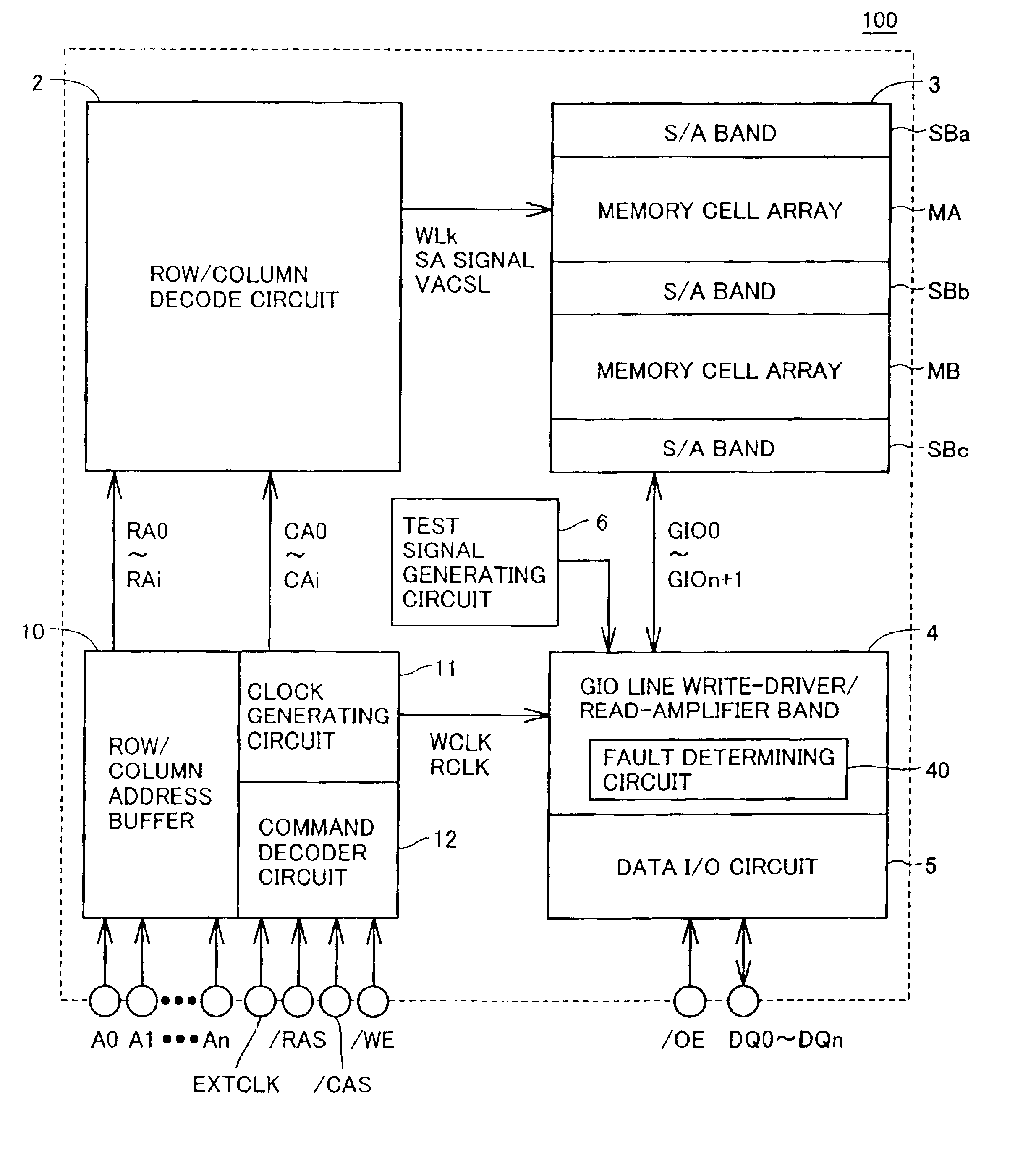
[0031]FIG. 1 is a block diagram showing a whole configuration of a semiconductor memory device 100 of a first embodiment of the invention.

[0032]Referring to FIG. 1, a semiconductor memory device 100 includes a row / column address buffer 10 taking in address signals A0-An, a clock generating circuit 11 which receives an external clock signal EXTCLK, and generates a clock signal determining timing of an internal operation, and a command decoder 12 which generates an internal control signal in response to an external control signal.

[0033]Row / column address buffer 10 predecodes a row-related address signal, and outputs row address signals RA0-RAi. Further, row / column address buffer 10 predecodes a column-related address signal to output column address signals CA0-CAi.

[0034]Clock generating circuit 11 generates, an internal clock signal int.CLK, a write clock signal WCLK for a write operation and a read clock RCLK for a read operation.

[0035]Command decoder 12 receives a ...

second embodiment

[Second Embodiment]

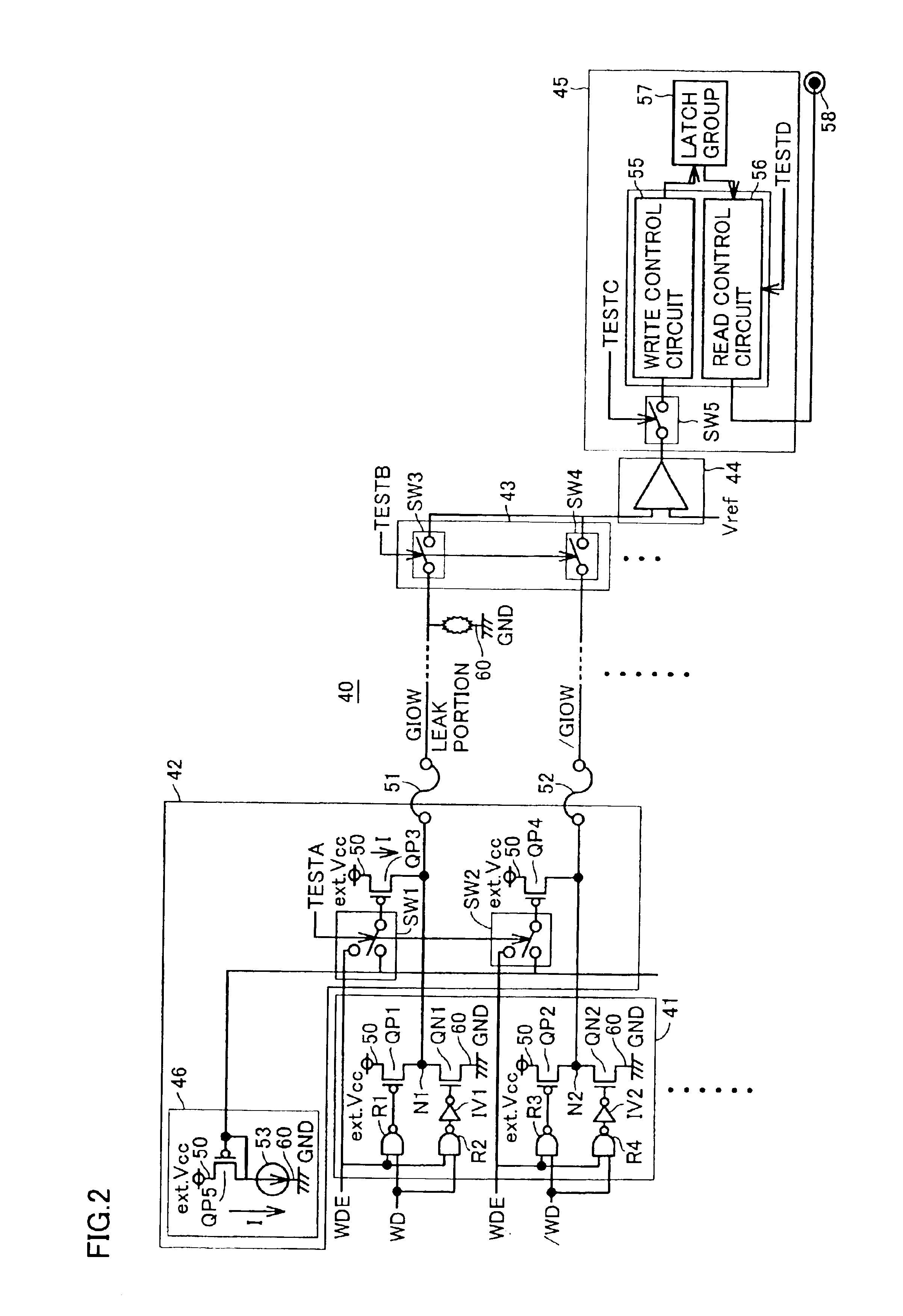
[0083]In the first embodiment described above, write data lines GIOW and / GIOW are precharged to H-level when operating the faulty determining circuit.

[0084]In a second embodiment, write data lines GIOW and / GIOW are precharged to L-level when operating the faulty determining circuit, as described below.

[0085]FIG. 4 is a block diagram showing a configuration of the fault determining circuit in the second embodiment of the invention.

[0086]Referring to FIG. 4, a fault determining circuit 70 differs from fault determining circuit 40 shown in FIG. 2 in that a potential supply circuit 72 is employed instead of potential supply circuit 42. Further, inverters IV3 and IV4 are added.

[0087]Potential supply circuit 72 includes N-channel MOS transistors QN3 and QN4, switching elements SW6 and SW7, and a reference current generating circuit 71.

[0088]Reference current generating circuit 71 includes an N-channel MOS transistor QN5 and a constant current supply 54.

[0089]Transisto...

third embodiment

[Third Embodiment]

[0100]FIG. 5 is a block diagram showing a configuration of a fault determining circuit 80 in a third embodiment of the invention.

[0101]Referring to FIG. 5, fault determining circuit 80 differs from fault determining circuit 40 shown in FIG. 2 in that a potential supply circuit 81 is employed instead of write driver 41 and potential supply circuit 42.

[0102]Potential supply circuit 81 includes a driver circuit 82, a transistor forced operation circuit 83, logic gates R1-R4, and inverters IV1 and IV2.

[0103]Driver circuit 82 includes P-channel MOS transistors QP1 and QP2 as well as N-channel MOS transistors QN1 and QN2.

[0104]Transistors QP1 and QN1 are connected in series between external power supply node 50 and ground node 60. The gate of transistor QP1 is connected to a switching element SW8. The gate of transistor QN1 is connected to a switching element SW9. Connection node N1 between transistors QP1 and QN1 is connected to write data line GIOW via fuse element 51....


PUM


Abstract

A write-driver/read-amplifier circuit includes a write driver, a GIO equalize circuit and a read amplifier. When a current leaks from or to global data line, a signal applied to a logic gate attains L-level. As a result, the write driver and the GIO equalize circuit stop the operations so that a semiconductor memory device can prevent occurrence of an unnecessary leak current.

Description

BACKGROUND OF THE INVENTION[0001]1. Field of the Invention[0002]The present invention relates to a semiconductor memory device, and particularly to a semiconductor memory device having a plurality of signal lines for writing and reading data.[0003]2. Description of the Background Art[0004]In recent years, capacities of semiconductor memory devices such as dynamic random access memories have been increased. As a result, faults may occur in memory cells in a manufacturing step. Also, faults may occur in signal lines such as word lines, bit lines and data lines. In a conventional manner, defects in such signal lines are externally detected by a tester from outside the semiconductor memory device.[0005]In recent years, however, signal lines in semiconductor memory devices have been subminiaturized for increasing capacities of the semiconductor memory devices. According to a fault detecting method using an external tester, therefore, it is difficult to detect faults finely by checking si...

Claims


Application Information

Patent Timeline
Patent Type & Authority Patents(United States)
IPC IPC(8): G11C7/10G11C29/00G11C29/02G11C11/401G11C29/04G11C29/12
CPCG11C7/1048G11C7/1051G11C7/1069G11C7/1078G11C7/1096G11C29/02G11C29/025G11C29/848G11C29/83G11C2029/5006
Inventor OOISHI, TSUKASATANIZAKI, HIROAKI
Owner RENESAS ELECTRONICS CORP
Why Eureka
Try Eureka