III-nitride light-emitting devices with improved high-current efficiency

a technology of iiinitride and light-emitting devices, which is applied in the field of improving the quantum efficiency of iiinitride light-emitting devices, can solve the problems of reducing the confinement of holes and hence quantum efficiency, and the simulation is not physically realistic, so as to achieve the reduction of polarization, the effect of reducing the polarization and advantageously increasing the efficiency

Active Publication Date: 2005-09-13
LUMILEDS
View PDF3 Cites 51 Cited by
  • Summary
  • Abstract
  • Description
  • Claims
  • Application Information

AI Technical Summary

Benefits of technology

[0013]In one aspect of the invention, a light-emitting semiconductor device comprises a III-Nitride active region and a III-Nitride layer formed proximate to the active region and having a thickness that exceeds a critical thickness for relaxation of strain in the III-Nitride layer. The III-Nitride layer may be a carrier confinement layer, for example. The piezoelectric polarization in the III-Nitride layer may be reduced as a consequence of its thickness. The reduced polarization may result in an advantageous increase in the efficiency with which the device emits light.
[0014]In another aspect of the invention, a light-emitting semiconductor device comprises a III-Nitride light emitting layer, an InxAlyGa1-x-yN (0≦x≦1, 0≦y≦1, x+y≦1), and a spacer layer interposing the light emitting layer and the InxAlyGa1-x-yN layer. The spacer layer may advantageously space the InxAlyGa1-x-yN layer and any contaminants therein apart from the light emitting layer. The composition of the III-Nitride layer may be advantageously selected to determine a strength of an electric field in the III-Nitride layer and thereby increase the efficiency with which the device emits light.

Problems solved by technology

Hence, this simulation is not physically realistic.
Moreover, polarization fields in n-type hole confinement layers may similarly reduce hole confinement and hence quantum efficiency.

Method used


Image

  • III-nitride light-emitting devices with improved high-current efficiency
  • III-nitride light-emitting devices with improved high-current efficiency
  • III-nitride light-emitting devices with improved high-current efficiency

Examples


Embodiment Construction

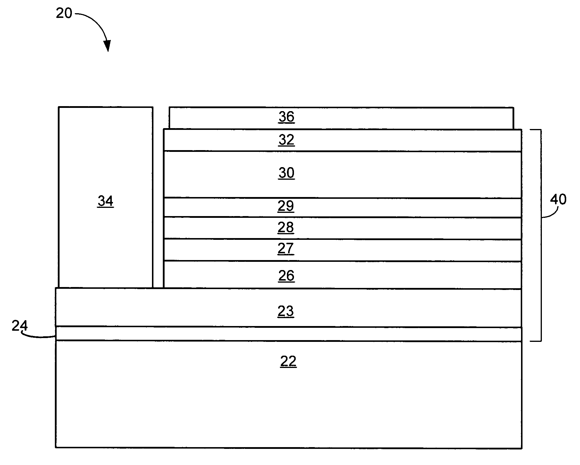
[0030]Several embodiments are disclosed in which polarization fields are reduced in electron and / or hole confinement layers in III-Nitride light-emitting devices. Confinement of electrons and holes in the active regions of these devices may thereby be improved. This can result in devices with improved quantum efficiency. The III-Nitride light-emitting devices described may be, for example, light-emitting diodes or laser diodes.

[0031]In one embodiment (FIG. 2), a III-N based LED 20 includes a sapphire substrate 22, a nucleation layer 24, an optional n-type III-Nitride contact layer, an n-type III-Nitride hole confinement layer 26, a III-Nitride active region 28, a p-type III-Nitride electron confinement layer 30, and an optional p-type III-Nitride contact layer 32. Active region 28 includes one or more quantum well layers and one or more barrier layers. Active region 28 may be spaced apart from electron confinement layer 30, hole confinement layer 26, or both by optional spacer layer...


PUM


Abstract

A light-emitting semiconductor device comprises a III-Nitride active region and a III-Nitride layer formed proximate to the active region and having a thickness that exceeds a critical thickness for relaxation of strain in the III-Nitride layer. The III-Nitride layer may be a carrier confinement layer, for example. In another aspect of the invention, a light-emitting semiconductor device comprises a III-Nitride light emitting layer, an InxAlyGa1-x-yN (0≦x≦1, 0≦y≦1, x+y≦1), and a spacer layer interposing the light emitting layer and the InxAlyGa1-x-yN layer. The spacer layer may advantageously space the InxAlyGa1-x-yN layer and any contaminants therein apart from the light emitting layer. The composition of the III-Nitride layer may be advantageously selected to determine a strength of an electric field in the III-Nitride layer and thereby increase the efficiency with which the device emits light.

Description

BACKGROUND[0001]1. Field of Invention[0002]The present invention relates to semiconductor light-emitting devices and, more particularly, to improving the quantum efficiency of III-Nitride light-emitting devices.[0003]2. Description of Related Art[0004]III-Nitride light-emitting devices are based on semiconducting alloys of nitrogen with elements from group III of the periodic table. Examples of such III-Nitride devices include InxAlyGa1-x-yN (0≦x≦1, 0≦y≦1, x+y≦1) based light emitting diodes (LEDs) and laser diodes (LDs). Such III-Nitride light emitting devices are commercially valuable high brightness sources of, for example, ultraviolet, blue, and green light.[0005]InxAlyGa1-x-yN crystals such as those from which InxAlyGa1-x-yN light emitting devices are formed typically adopt the wurtzite crystal structure and are consequently polarized even when not externally biased. The two types of polarization that are significant for III-Nitride light-emitting devices are the spontaneous and...

Claims


Application Information

Patent Timeline
Patent Type & Authority Patents(United States)
IPC IPC(8): H01L33/00H01L33/32
CPCH01L33/32
Inventor GARDNER, NATHAN F.KOCOT, CHRISTOPHER P.STOCKMAN, STEPHEN A.
Owner LUMILEDS
Why Eureka
Try Eureka