

Generation of a library of periodic grating diffraction signals
- Summary
- Abstract
- Description
- Claims
- Application Information
AI Technical Summary
Benefits of technology
Problems solved by technology
Method used
Image

Examples
Embodiment Construction
[0022]The following description sets forth numerous specific configurations, parameters, and the like. It should be recognized, however, that such description is not intended as a limitation on the scope of the present invention, but is instead provided to provide a better description of exemplary embodiments.
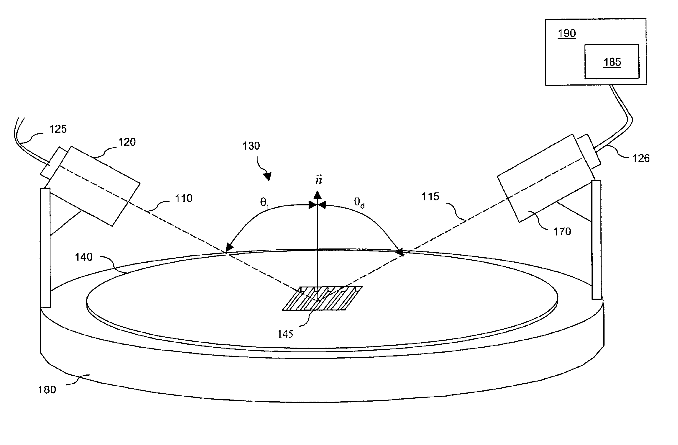
[0023]With reference to FIG. 1, a periodic grating 145 is depicted on a semiconductor wafer 140. As depicted in FIG. 1, wafer 140 is disposed on a process plate 180, which can include a chill plate, a hot plate, a developer module, and the like. Alternatively, wafer 140 can also be disposed on a wafer track, in the end chamber of an etcher, in an end-station or metrology station, in a chemical mechanical polishing tool, and the like.
[0024]As described earlier, periodic grating 145 can be formed proximate to or within an operating structure formed on wafer 140. For example, periodic grating 145 can be formed adjacent a transistor formed on wafer 140. Alternatively, periodic grat...
PUM
 Abstract
Description
Claims
Application Information