Method and apparatus for the analysis of scratches on semiconductor wafers

a technology for semiconductor wafers and scratches, applied in the direction of semiconductor/solid-state device testing/measurement, instruments, image enhancement, etc., can solve the problems of affecting the quality of semiconductor wafers, so as to reduce the cost of process installation, the effect of rapid and simple determination of process installation and scratching

Inactive Publication Date: 2005-09-13
POLARIS INNOVATIONS LTD
View PDF4 Cites 3 Cited by
  • Summary
  • Abstract
  • Description
  • Claims
  • Application Information

AI Technical Summary

Benefits of technology

[0011]This process according to the invention of searching for scratch causes on wafers makes it possible to rapidly and simply determine a process installation causing a scratch. As a result, there is no need for a complicated search for causes by installation correlation in the context of a batch comparison and complicated test runs with bare slices. At the same time, it is possible largely to dispense with a production installation stop during wafer fabrication and thus to avoid capacity losses through additional installation monitoring.
[0012]According to the invention, it is preferred to determine the parameter value identifying the scratch position and the scratch course on the semiconductor wafer surface in such a way that a straight line for the approximation of the scratch course is defined through the two end points of the detected scratch and the perpendicular distance between the center point of the semiconductor wafer slice and the straight line defining the scratch course is determined as the parameter value. This procedure enables a rapid and simple definition of a parameter for the correlation of scratches with process installations. The complexity for determining the parameter and thus the subsequently required comparison complexity for defining the installation causing the scratch can be reduced to a minimum. The mathematical complexity for defining the scratch parameter is minimal.
[0013]This applies in particular when, according to a preferred embodiment, for determining the perpendicular distance—defining the parameter value—between the center point of the semiconductor wafer slice and the straight line defining the scratch course, a procedure is chosen in which three points are determined on a circle circumference of the semiconductor slice, in which case two of the three points correspond to the end points of the scratch essentially tangentially lengthened on the circle circumference. Defining three points makes it possible to rapidly and simply calculate the wafer center point and radius and from the latter, in turn, the perpendicular distance of the straight line representing the scratch from a simple three-point coordinate detection. This procedure provides for a particularly simple and rapid detection of scratches on wafer surfaces.

Problems solved by technology

During this transfer of the semiconductor slices or of the batches with semiconductor slice surfaces, defects may arise on the semiconductor slices.
According to experience, 0.1% of the wafers are damaged by the handling of the wafers in the process installations or during the transport between the process installations.
In particular, the handling units often cause large scratches on the rear sides of the wafers during the transfer of the wafers, which scratches may bring about wafer fractures and thus a stoppage of the process installation.
Such a stoppage of the process installations then leads to the outage of fabrication capacity and at the same time to the loss of the wafer.
Defects caused by the process installations are also increasingly gaining in importance because the diameters of the semiconductor slices, and thus the risk of fracture, are increasing.
However, such installation correlation proves to be difficult in particular when a fault image occurs only at a small number of wafers.
However, this is time-consuming and expensive and furthermore leads to a production installation stop during chip fabrication.

Method used


Image

  • Method and apparatus for the analysis of scratches on semiconductor wafers
  • Method and apparatus for the analysis of scratches on semiconductor wafers

Examples


Embodiment Construction

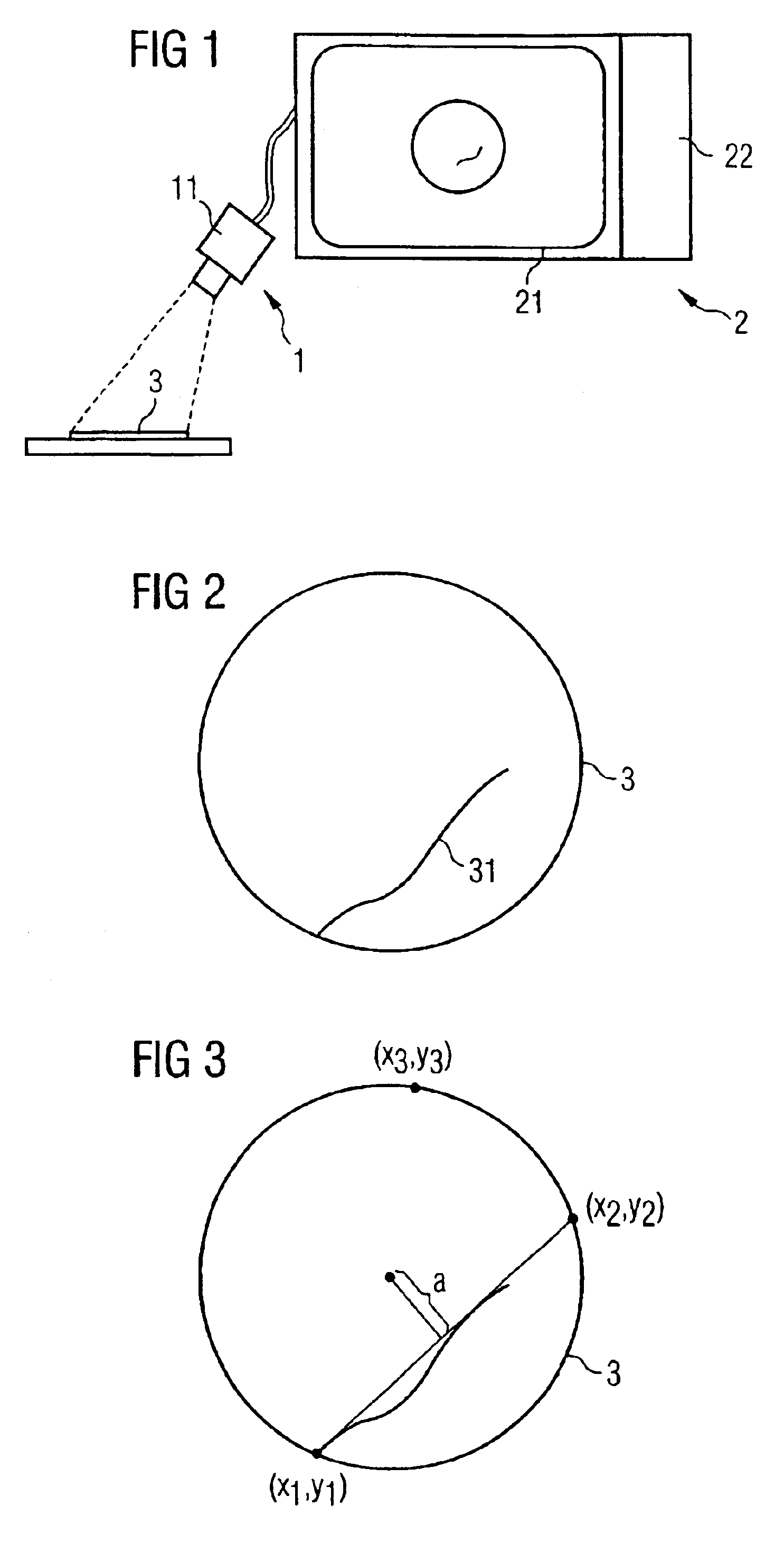
[0018]The apparatus according to the invention for scratch analysis is composed of a surface scanning device 1 and an analysis device 2 with screen 21. The scanning device 1 is preferably an optical scanning unit for automatically scanning a wafer surface 3. In this case, as is illustrated in FIG. 1, the wafer surface 3 is preferably detected optically by means of a camera 11 in a pass, in order not to obstruct the wafer flow during chip fabrication. However, instead of an optical detection, as shown in FIG. 1, it is possible to use any known method for scanning a surface. Scanning data are supplied to the analysis device 2 by the scanning device 1, which analysis device represents the scanned wafer surface on a screen 21. The wafer surface 3 is reproduced in enlarged fashion in FIG. 2.

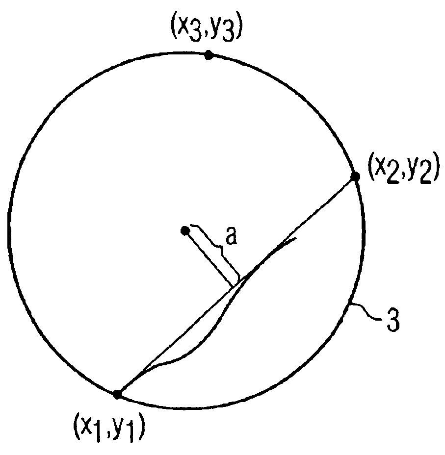
[0019]FIG. 2 shows that there is a long scratch 31 on the wafer surface 3. In order to determine the cause of this scratch 31, according to the invention, in the data processing unit 2, a parameter id...


PUM

PropertyMeasurementUnit
lengthaaaaaaaaaa
distanceaaaaaaaaaa
circumferenceaaaaaaaaaa

Abstract

For the analysis of scratches on semiconductor wafers, the semiconductor wafer surface is detected and a possible scratch position or a scratch course on the semiconductor surface is determined, in which case a parameter value identifying the scratch is determined from the scratch position and the scratch course and this parameter value that has been determined is correlated with comparison parameter values, which identify installation-specific scratch positions and scratch courses, in order to determine an installation causing the scratch.

Description

CROSS-REFERENCE TO RELATED APPLICATIONS[0001]This application claims foreign priority benefits under 35 U.S.C. §119 to co-pending German patent application 102 60 817.2-52, filed Dec. 23, 2002. This related patent application is herein incorporated by reference in its entirety.BACKGROUND OF THE INVENTION[0002]1. Field of the Invention[0003]The invention relates to a method and an apparatus for the analysis of scratches on semiconductor wafers.[0004]2. Description of the Related Art[0005]Electronics is nowadays dominated by microelectronic components with integrated circuits. Such integrated circuits represent a functional unit, which are characterized by a multiplicity of electronic functional elements having dimensions in the micron and sub-micron range and which are electrically and mechanically inseparably connected to one another. The electronic functional elements are realized on a common semiconductor substrate.[0006]The fabrication of integrated circuits is essentially subdiv...

Claims


Application Information

Patent Timeline
Patent Type & Authority Patents(United States)
IPC IPC(8): G01N21/88G01N21/95H01L21/66G06T7/00
CPCG01N21/95G06T7/0004H01L22/20G06T2207/30148
Inventor BRASACK, INGOBECKMANN, MARCO
Owner POLARIS INNOVATIONS LTD
Why Eureka
Try Eureka