Method of making a nanoscale electronic device

a technology of electronic devices and nano-scale, applied in the direction of material nanotechnology, semiconductor devices, electrical devices, etc., can solve the problems of increasing processing power and speed, devices present numerous difficulties in manufacturing, lithography and indeed physical laws, and current cmos transistors cannot be easily scaled to these dimensions

Inactive Publication Date: 2005-09-20
RICE UNIV
View PDF5 Cites 14 Cited by
  • Summary
  • Abstract
  • Description
  • Claims
  • Application Information

AI Technical Summary

Benefits of technology

[0020]Thus, the present invention solves the problem of making a device wherein at least two conductors or semiconductors form a nanoscale gap. In notable contrast to some prior art wherein the addition of electrical contacts takes place both before and after formation of a delicate organic component, the present method completes

Problems solved by technology

In the case of integrated circuits, reduced device size increases the number of transistors and decreases the distance between them collectively resulting in increases in processing power and speed.
Such devices present numerous difficulties with respect to manufacturing, lithography and indeed physical laws that make the use of silicon transistors at the nanoscale subject to quantum tunneling effects.
Because of these problems current CMOS transistors cannot easily be scaled to these dimensions.
It remains a significant challenge to squeeze high performance from transistors of remarkably small dimensions; in particular, retaining charge in capacitors of diminishing area and reducing refresh frequencies represent nontrivial problems in the art.
The major problem with fine scale lithography is that the wafer on which the devices are built must be aligned to within a small fraction of the size of the device features in at least two dimensions for several successive stages of lithography, followed by etching or deposition to build the devices.
This level of control does not scale well as device sizes are reduced to nanometer scale dimensions.
The main problem with direc

Method used


Image

  • Method of making a nanoscale electronic device
  • Method of making a nanoscale electronic device
  • Method of making a nanoscale electronic device

Examples


Embodiment Construction

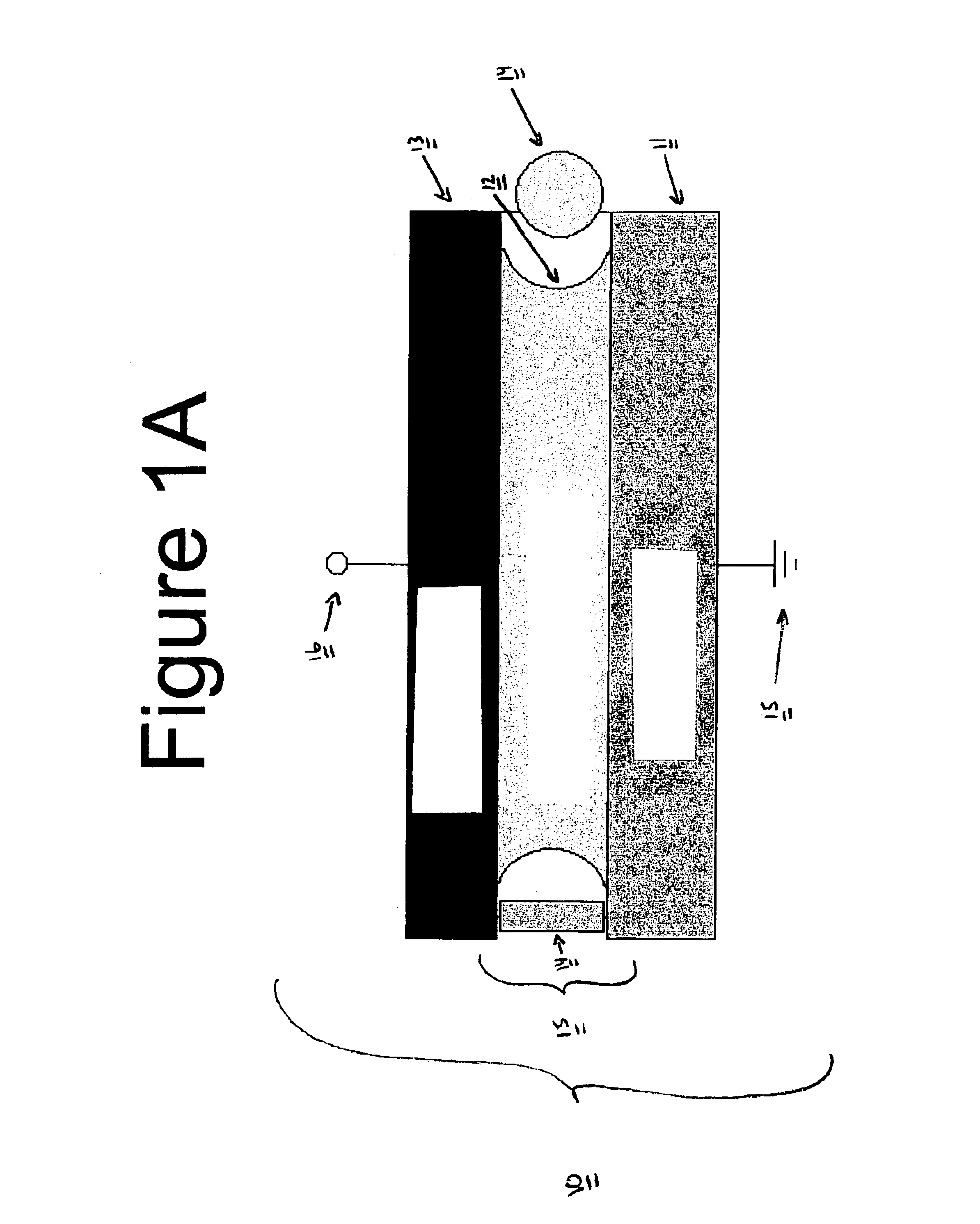
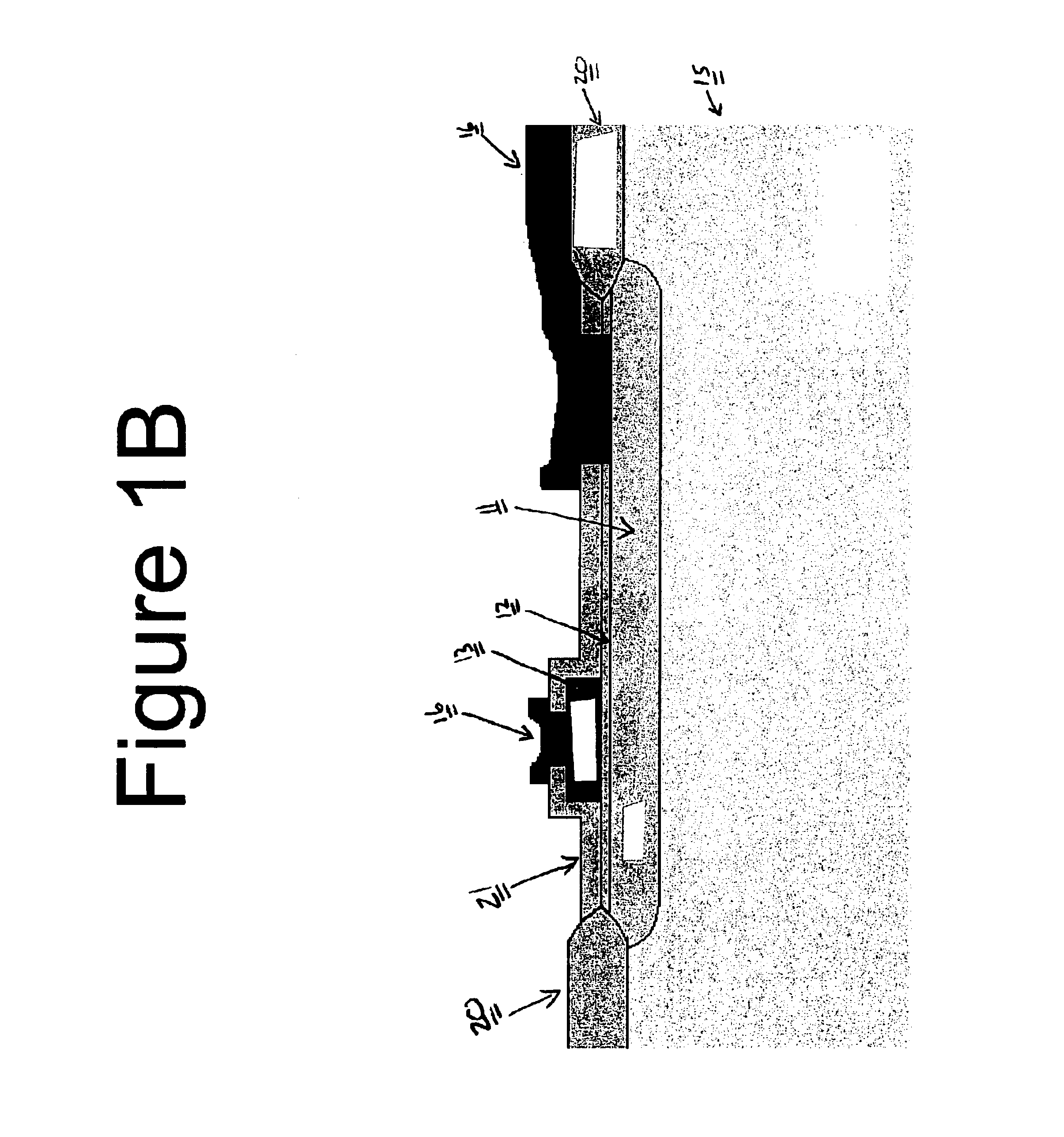
[0022]The present method permits for the creation of electronic devices of nanoscale dimensions. Specifically, the devices made will feature a gap that is between about 0.1 nm and about 100 nm in width. Furthermore, the present method is less susceptible to produce devices that are inoperable by virtue of electrical shorts introduced during the method of making. As described above, some previously employed methods suffer from the tendency to provide a high number of defective devices. This can, in one aspect, be attributed to the inherent assembly order. In those cases in which addition of a second electrical contact is performed after and atop a molecular electronic component, those methods have had the potential drawback that the integrity of the delicate molecular electronic component is often compromised by addition of a second electrical contact. Indeed, the yield of such devices may be less than 5%. Please see for example “Molecular Electronics: Commercial Insights, Chemistry,...


PUM


Abstract

The present invention relates to a method of making a nanoscale electronic device wherein said device comprises a gap between about 0.1 nm and about 100 nm between at least two conductors, semiconductors or the combination thereof. The method features complete assembly of electrical contacts before addition of a molecular component thereby preserving the integrity of the molecular electronic component and maintaining a well-formed gap. The gap produced is within the nanoscale regime, has uniform width and is further characterized by surfaces that are uniformly smooth.

Description

CROSS-REFERENCE TO RELATED APPLICATIONS[0001]This nonprovisional patent application claims the benefit of U.S. Provisional Patent Application Ser. No. 60 / 380,000, filed May 13, 2002.STATEMENT REGARDING FEDERALLY SPONSORED RESEARCH OR DEVELOPMENT[0002]The research carried out in connection with this invention was funded by Defense Advanced Research Projects Agency (DARPA) administered by the Office of Naval Research (ONR), Grant No. N00014-01-1-0657.FIELD OF THE INVENTION[0003]The present invention relates to a method of making a nanoscale electronic device wherein said device comprises a gap between about 0.1 nm and about 100 nm between at least two conductors, semiconductors or the combination thereof. The present method comprises, in part, depositing an insulating dielectric onto a conductor or semiconductor in a manner sufficient to precisely obtain a uniformly thin and smooth layer of said insulating dielectric. The method further comprises depositing a quantity of another condu...

Claims


Application Information

Patent Timeline
IPC IPC(8): H01L21/28H01L21/02H01L21/70H01L21/336H01L21/44H01L21/8238B82BH01L51/00
CPCB82Y10/00B82Y30/00H01L51/0595Y10S977/932H10K10/701
Inventor PANG, HARRY F.TOUR, JAMES M.
Owner RICE UNIV
Why Eureka
Try Eureka