
Crystal oscillation device and electronic device using the same

a crystal oscillation device and crystal oscillation technology, applied in the direction of printed circuit non-printed electric components association, pulse technique, final product manufacture, etc., can solve the problems of difficult to reduce the operation cost, difficult to mount circuit components, and difficult to reduce the cost, so as to achieve small cost

Active Publication Date: 2005-09-20
MURATA MFG CO LTD
View PDF4 Cites 13 Cited by
  • Summary
  • Abstract
  • Description
  • Claims
  • Application Information

AI Technical Summary

Benefits of technology

[0012]To overcome the problems described above, preferred embodiments of the present invention provide a small, low-profile, and low-cost crystal oscillation device that is rarely damaged by a drop impact or other damaging impacts and to provide an electronic device using the crystal oscillation device.
[0017]The resulting crystal oscillation device according to preferred embodiments of the present invention has greatly reduced size and cost.
[0018]According to another preferred embodiment of the present invention, an electronic device includes the above-described crystal oscillation device, such that the performance of the electronic device is greatly improved.

Problems solved by technology

In Japanese Unexamined Patent Application Publication No. 2001-177345, because the circuit board is formed of a ceramic box, it is difficult to reduce the cost thereof.
Moreover, it is much more difficult to mount circuit components on the bottom of the recess of the box-shaped circuit board than to mount the components on a flat board, and it is also difficult to reduce the operation cost.
In addition, the area of the circuit board must be increased corresponding to the thicknesses of the four side walls of the box-shaped circuit board, and this hinders size reduction of the crystal oscillation device.
In Japanese Unexamined Patent Application Publication No. 2002-84138, because the external terminals protrude from the case of the crystal oscillator, the cost of the crystal oscillator is increased.
In Japanese Unexamined Patent Application Publication No. 2002-64333, because the crystal oscillator is supported only by the columnar members, the strength is insufficient.
While the strength can be increased by forming the columnar members integrally with the package of the crystal oscillator, the cost of the package is increased.

Method used


Image

  • Crystal oscillation device and electronic device using the same
  • Crystal oscillation device and electronic device using the same
  • Crystal oscillation device and electronic device using the same

Examples


Embodiment Construction

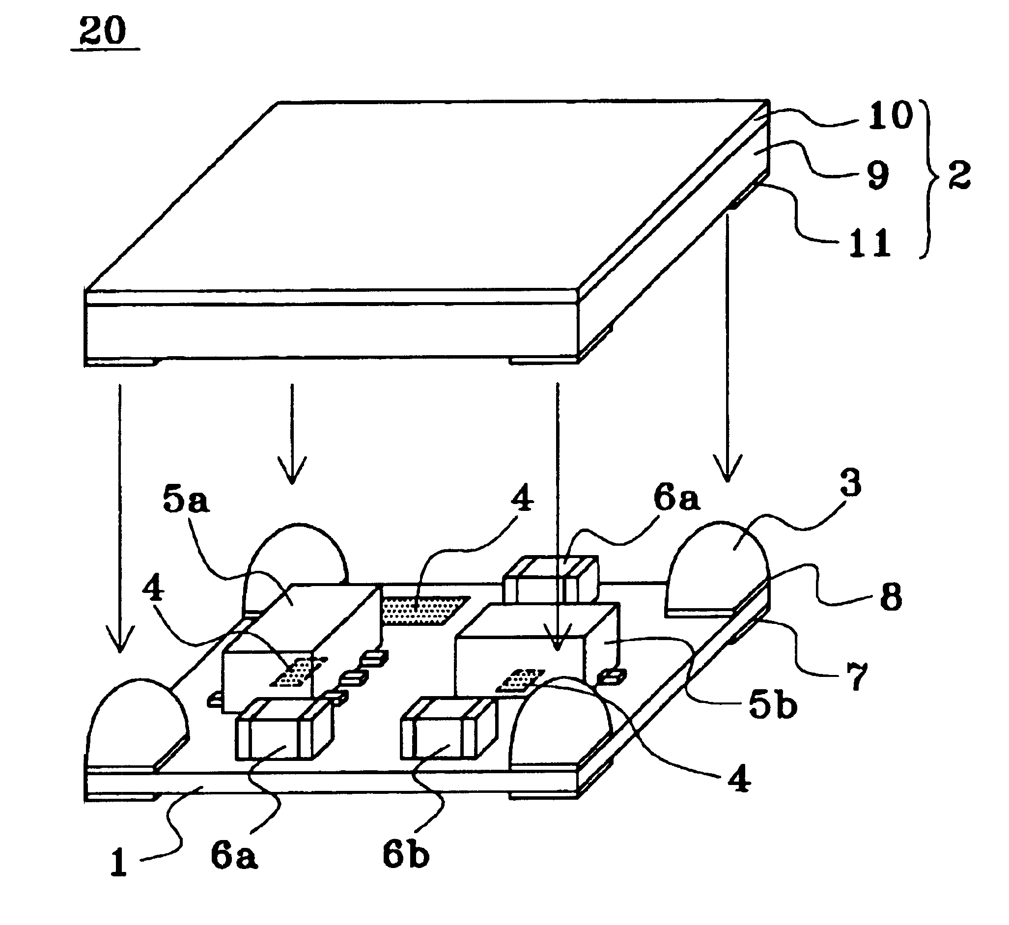
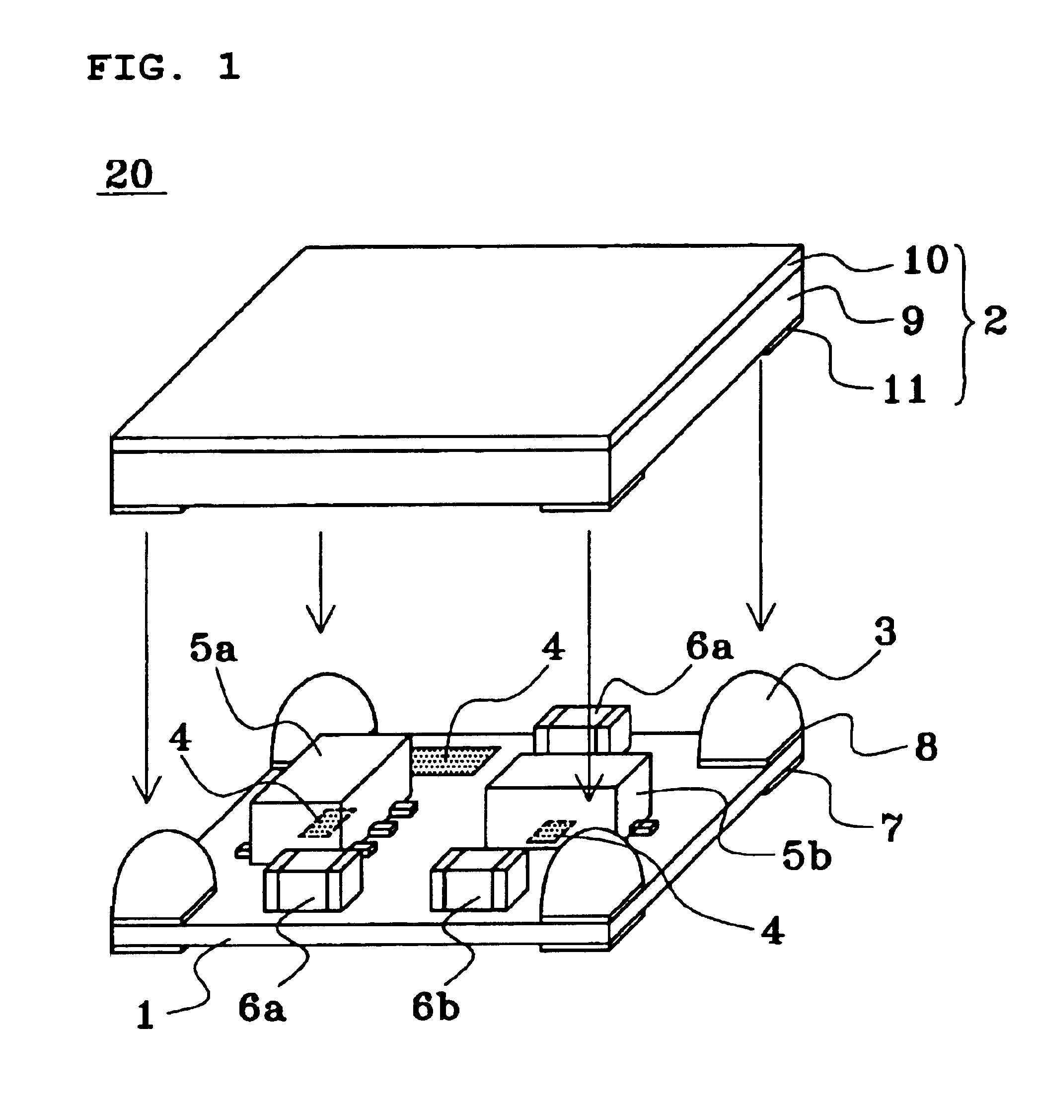
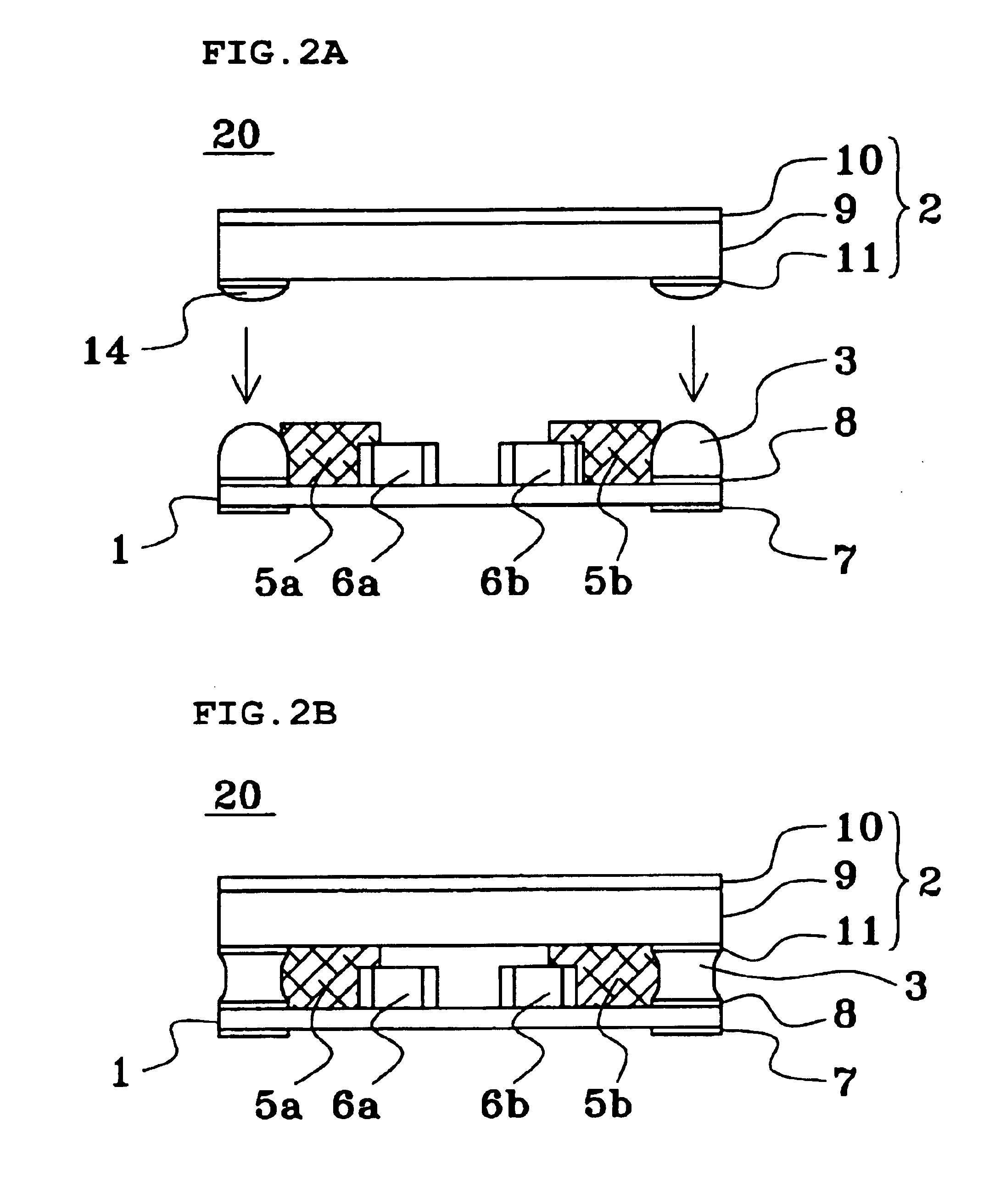
[0027]FIG. 1 is an exploded perspective view of a crystal oscillation device according to the first preferred embodiment, FIGS. 2A and 2B are side views of the crystal oscillation device, and FIGS. 3A and 3B are a cross-sectional view and a bottom view, respectively, of the crystal oscillation device. Referring to FIGS. 1, 2A, and 2B, a crystal oscillation device 20 preferably has a configuration in which a packaged oscillator 2 is mounted on a flat thin circuit board 1.

[0028]Circuit components, such as a transistor 5a, a varicap diode 5b, chip capacitors 6a, and a thermistor 6b, are mounted on the circuit board 1. The transistor 5a and the varicap diode 5b are preferably molded resin components, are substantially equal in height, and have a flat top surface. Printed resistors 4 are also preferably formed as circuit components on the circuit board 1. Some of the printed resistors 4 are provided under the transistor 5a and the varicap diode 5b. These circuit components form an oscill...


PUM


Abstract

A crystal oscillation device includes a crystal oscillator including a package with first connecting electrodes provided on a flat bottom surface mounted on a flat, thin circuit board. Circuit components and second connecting electrodes provided in one-to-one correspondence with the first connecting electrodes are mounted on one principal surface of the circuit board. The crystal oscillator is supported by top surfaces of a transistor and a varicap diode that are the highest among the circuit components mounted on the circuit board. The crystal oscillator and the circuit board are electrically connected with solder provided between the first and second connecting electrodes. The solder also attracts the crystal oscillator toward the circuit board.

Description

BACKGROUND OF THE INVENTION[0001]1. Field of the Invention[0002]The present invention relates to a crystal oscillation device and an electronic device, and more particularly, to a crystal oscillation device, for example, used as a reference signal source in a PLL (Phase-Locked Loop) circuit included in a RF (Radio Frequency) circuit of a portable telephone and to an electronic device including the crystal oscillation device.[0003]2. Description of the Related Art[0004]In a conventional crystal oscillation device used as a reference signal source, a crystal oscillator is used as a resonator, and circuit components that define an oscillation circuit, a temperature-compensating circuit, and other suitable components are combined with the crystal oscillator. The conventional crystal oscillator normally has a structure in which a crystal strip with an electrode is hermetically mounted in a package made of ceramic or other suitable material. The circuit components need to be mounted on a ...

Claims


Application Information

Patent Timeline
IPC IPC(8): H05K1/18H05K3/34H05K3/30H03B5/32
CPCH05K1/181H05K3/303H05K3/3442H05K2201/10075H05K2201/10166H05K2201/10174H05K2201/10515H05K2201/10727H05K2201/2036Y02P70/50
Inventor TAKEMURA, TADAJIOKUMURA, YASUSHI
Owner MURATA MFG CO LTD
Learn More