Method of evaluating core based system-on-a-chip (SoC) and structure of SoC incorporating same

a technology of core based system and chip, which is applied in the direction of software simulation/interpretation/emulation, instruments, program control, etc., can solve the problems of major difficulty in determining the functional correctness of prototype silicon, the complexity of these chips is far too complex to be tested by conventional means, and the limited observability and controllability of individual cores

Inactive Publication Date: 2005-09-20
ADVANTEST CORP
View PDF4 Cites 24 Cited by
  • Summary
  • Abstract
  • Description
  • Claims
  • Application Information

AI Technical Summary

Benefits of technology

[0019]According to the present invention, the silicon debug method does not require any additional test circuitry. It does not require any design modification in the chip design, there is no performance penalty and core test pattern can be app

Problems solved by technology

While such system-chips serve for broad applications, the complexity of these chips is far too complex to be tested by conventional means.
In addition to the difficulties in the production testing, these SoCs also present major difficulty in determining their functional correctness when prototype silicon is manufactured.
The primary cause of the difficulty is limited observability and controllability of individual cores.
The major drawbacks in these methods are that they require extra logic that increases chip size and hence the cost; and performance penalty because of the wrapper at the core I/Os.
An example of such performance penalty includes signal propagation delays in SoC because of the additional circuit c

Method used


Image

  • Method of evaluating core based system-on-a-chip (SoC) and structure of SoC incorporating same
  • Method of evaluating core based system-on-a-chip (SoC) and structure of SoC incorporating same
  • Method of evaluating core based system-on-a-chip (SoC) and structure of SoC incorporating same

Examples


Embodiment Construction

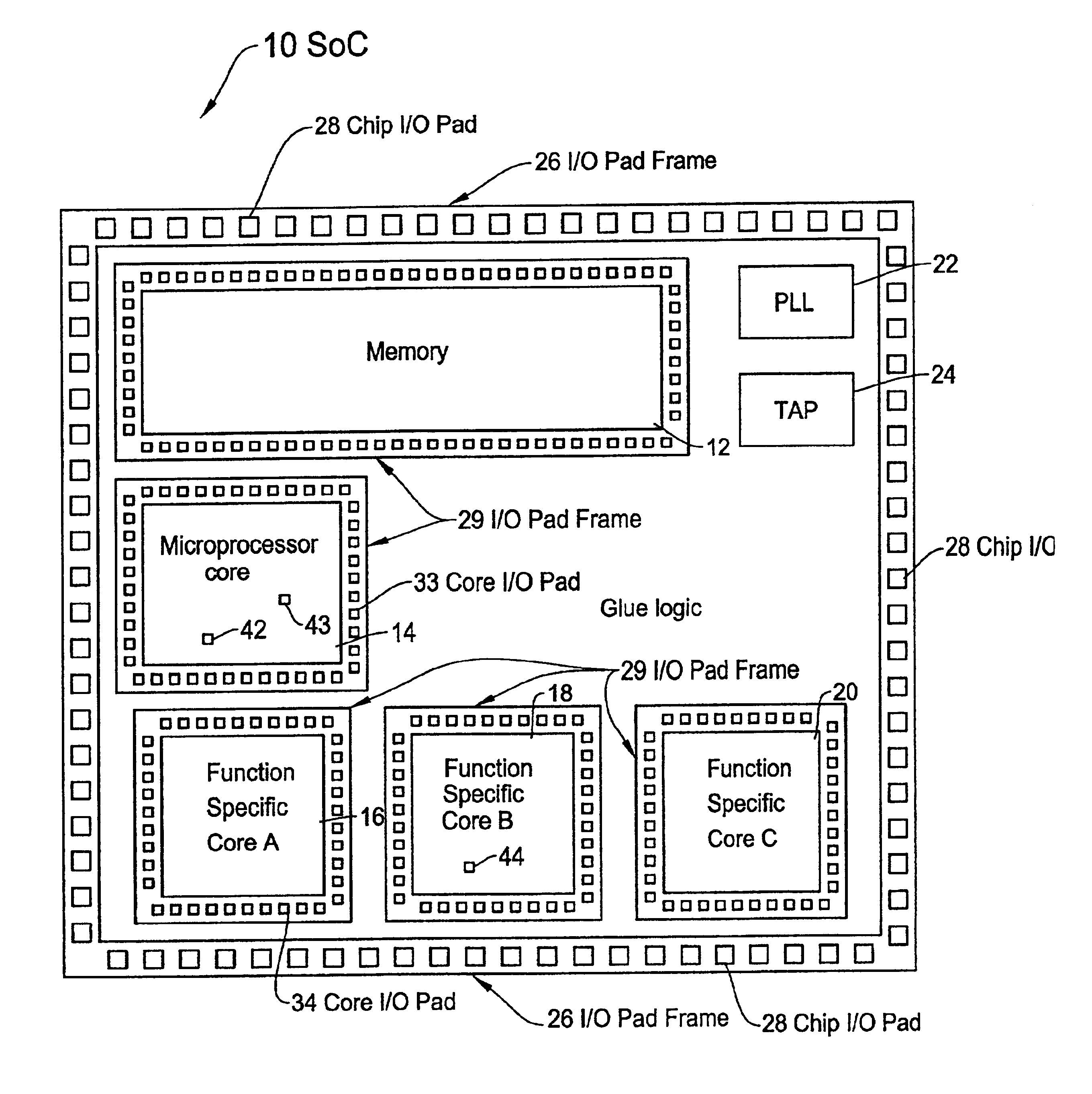
[0029]Referring now to FIGS. 3 and 4, there is shown a basic concept in the present invention to establish an I / O interface for each core that can be directly accessible by traditional contact probes. In the present invention, the I / O interface of an individual core can be used for test signal application and response signal observation. Consequently, it is able to apply a core test pattern (rather than a chip test pattern) directly to a particular core, i.e., it is only necessary to access the I / Os of the core.

[0030]More specifically, as shown in FIGS. 3 and 4, the I / O pad-frame of each core is duplicated in the top-level metal during the prototype manufacturing. As noted above with reference to the prior art technology, the top-level metal layer of the I / O pad frame is generally used only for routing power lines, and lower level metal layers are used for routing signals including I / Os. Thus, it is not possible to access the individual core through the I / O pad frame of individual c...


PUM


Abstract

A method of debugging an individual core in core based system-on-a-chip (SOC) ICs with high accuracy and observability, and a structure of SOC incorporating the method. The method includes the steps of building two or more metal layers of a pad frame for each core in an SoC while connecting I/O (input and output) pads on a lower metal layer to a top metal layer, thereby exposing all I/O pads and power pads on a surface of the top metal layer of the pad frame of each core, and applying test vector to each core through the I/O pads on the top metal layer of the core and evaluating response outputs of the core received through the I/O pads on the top metal layer.

Description

FIELD OF THE INVENTION[0001]This invention relates to a method of testing semiconductor devices, and more particularly, to a method of debugging design integrity of core based system-on-a-chip (SoC) ICs in a silicon form (silicon debug) with high accuracy and observability. The present invention also relates to a structure of SoC IC implementing the method of silicon debug.BACKGROUND OF THE INVENTION[0002]In recent several years, ASIC (Application Specific Integrated Circuit) technology has evolved from a chip-set philosophy to an embedded cores based system-on-a-chip (SoC). An SoC is an IC designed by stitching together multiple stand-alone VLSI designs (cores) to provide full functionality for an application. Namely, the SoCs are built using pre-designed models of complex functions known as “cores” (also known as Intellectual Property or IP) that serve a variety of applications. These cores are generally available either in high-level description language (HDL) such as in Verilog / ...

Claims


Application Information

Patent Timeline
IPC IPC(8): G01R31/3185G01R31/317G01R31/28
CPCG01R31/31704G01R31/31705G01R31/31724G01R31/3185G01R31/318508G01R31/318552H01L2924/0002H01L2924/00G01R31/28
Inventor RAJSUMAN, ROCHIT
Owner ADVANTEST CORP
Why Eureka
Try Eureka