Nonvolatile semiconductor memory device and method for operating the same

Inactive Publication Date: 2005-09-27
SONY CORP
View PDF5 Cites 64 Cited by
  • Summary
  • Abstract
  • Description
  • Claims
  • Application Information

AI Technical Summary

Benefits of technology

[0049]By either of the tunneling effects,

Problems solved by technology

When a leakage current path in locally generated in the tunneling insulating film, in an FG type, a large amount of charge easily leaks out through the leakage path and the charge retention characteristic declines.
As a result, in a MONOS type, the disadvantage of the degradation of the charge retention characteristic due to the reduction in thickness of the tunnel insulating film is not so serious as in an FG type.
When the tunneling insulating film is formed relatively thick, the write speed is in the range of 0.1 to 10 ms, which is still not sufficient.
A high speed is possible if the write speed alone is considered, but sufficiently high reliability and low voltages cannot be achieved.
In

Method used


Image

  • Nonvolatile semiconductor memory device and method for operating the same
  • Nonvolatile semiconductor memory device and method for operating the same
  • Nonvolatile semiconductor memory device and method for operating the same

Examples


first embodiment

[0072]The first embodiment relates to a virtual grounding NOR type nonvolatile semiconductor memory device.

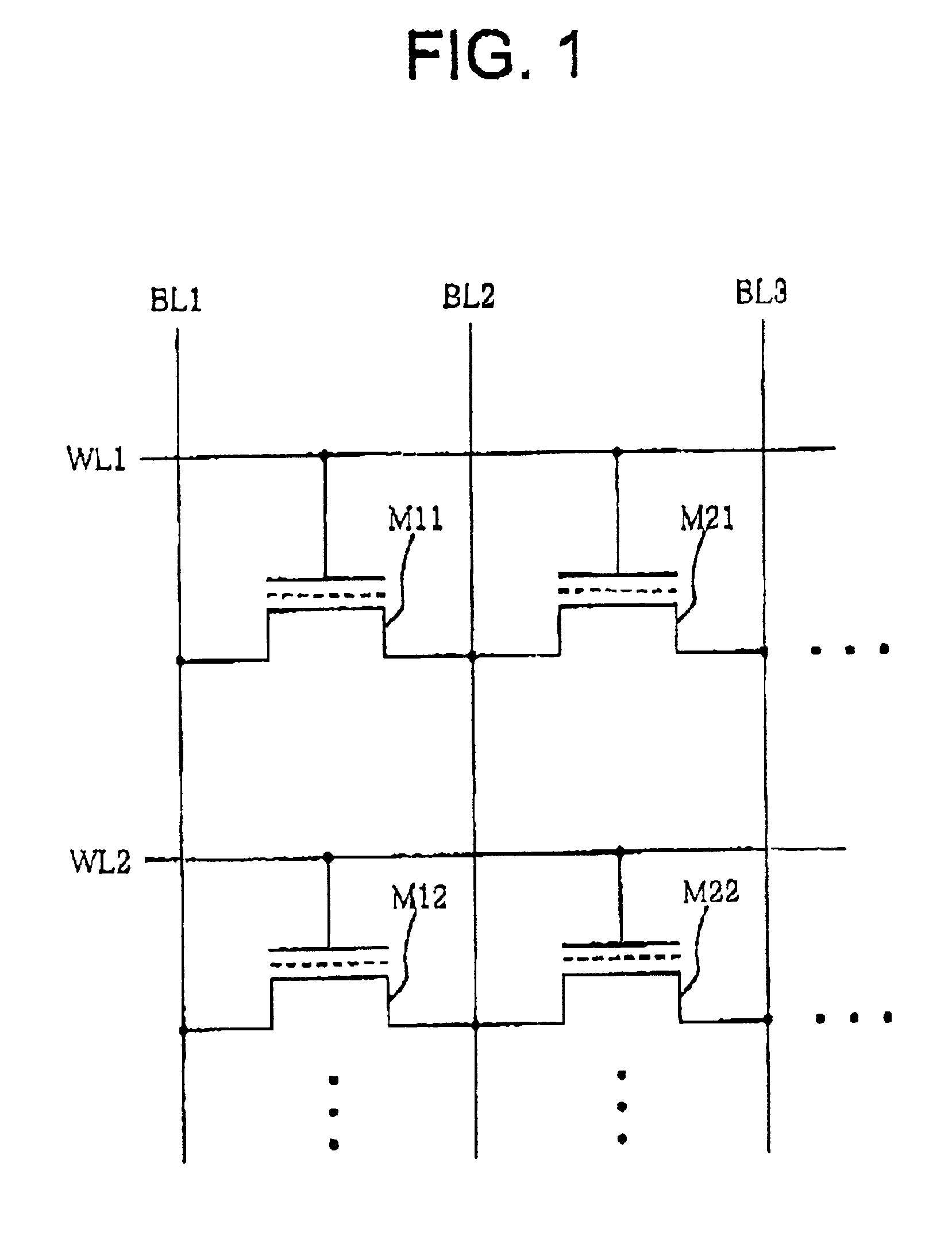
[0073]FIG. 1 is a circuit diagram of the configuration of a virtual grounding NOR type memory cell array.

[0074]In this memory cell array, each memory cell is comprised of a single memory transistor. For example, m×n memory transistors M11, M21, . . . , Mm1, M12, M22, . . . , M1n, . . . , Mmn are arranged like a matrix. Shown in FIG. 1 are only 2×2 memory transistors.

[0075]Each gate of memory transistors in one row is connected to the same word line. That is, in FIG. 1, gates of memory transistors belonging to the same row M11, M21, . . . , are connected to the word line WL1. While, gates of memory transistors belonging to the other row M12, M22, . . . , are connected to the word line WL2.

[0076]Each source of memory transistors is connected to the drain of a memory transistor adjacent at one side in the word direction. The drain of a memory transistor is connected to the source ...

second embodiment

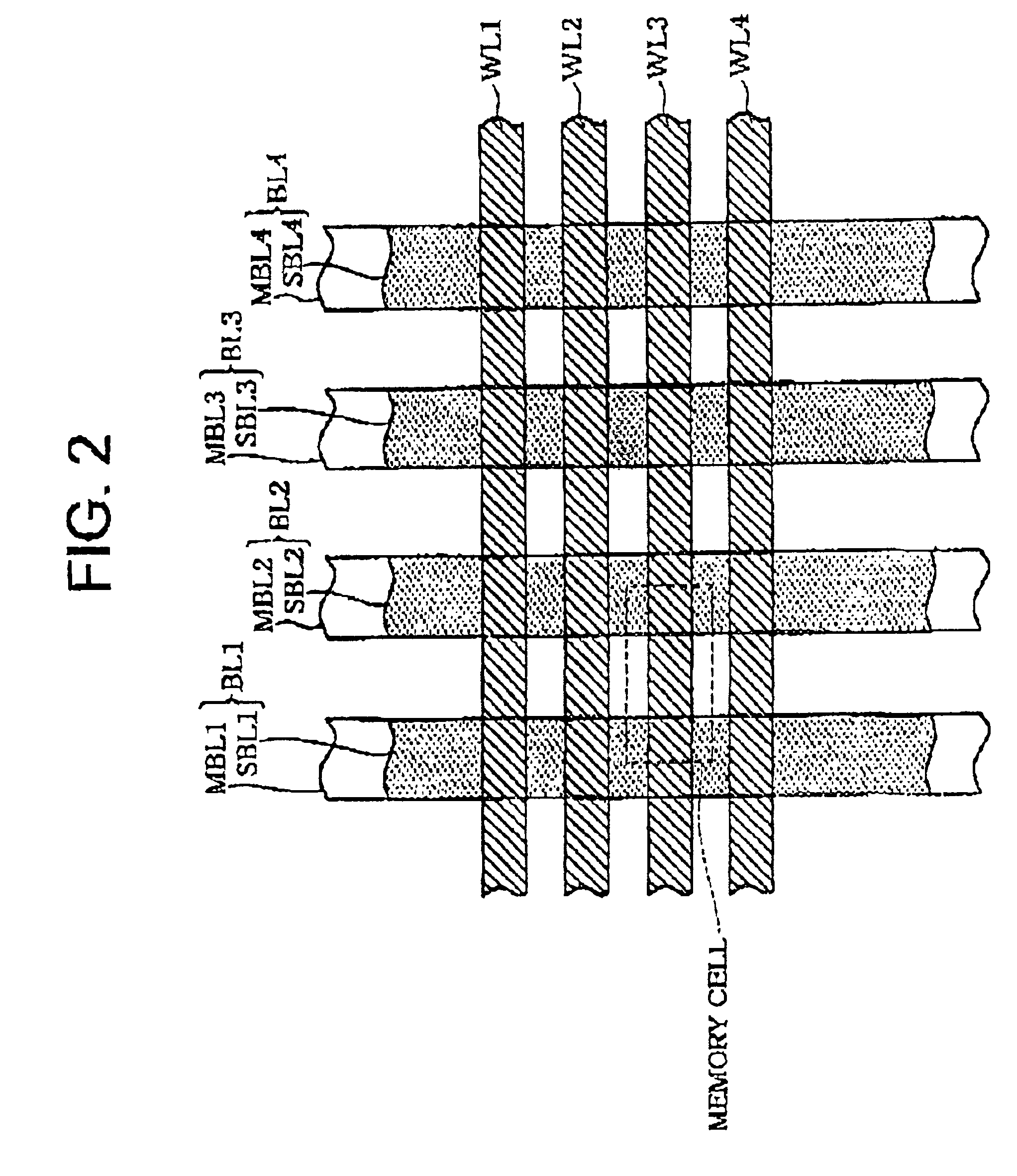
[0131]The second embodiment relates to a modification of the configuration of the gate insulating film of a memory transistor in a virtual grounding NOR type nonvolatile semiconductor memory device. Tho circuit diagram in FIG. 1 and the plain view in FIG. 2 are also applicable to the second embodiment.

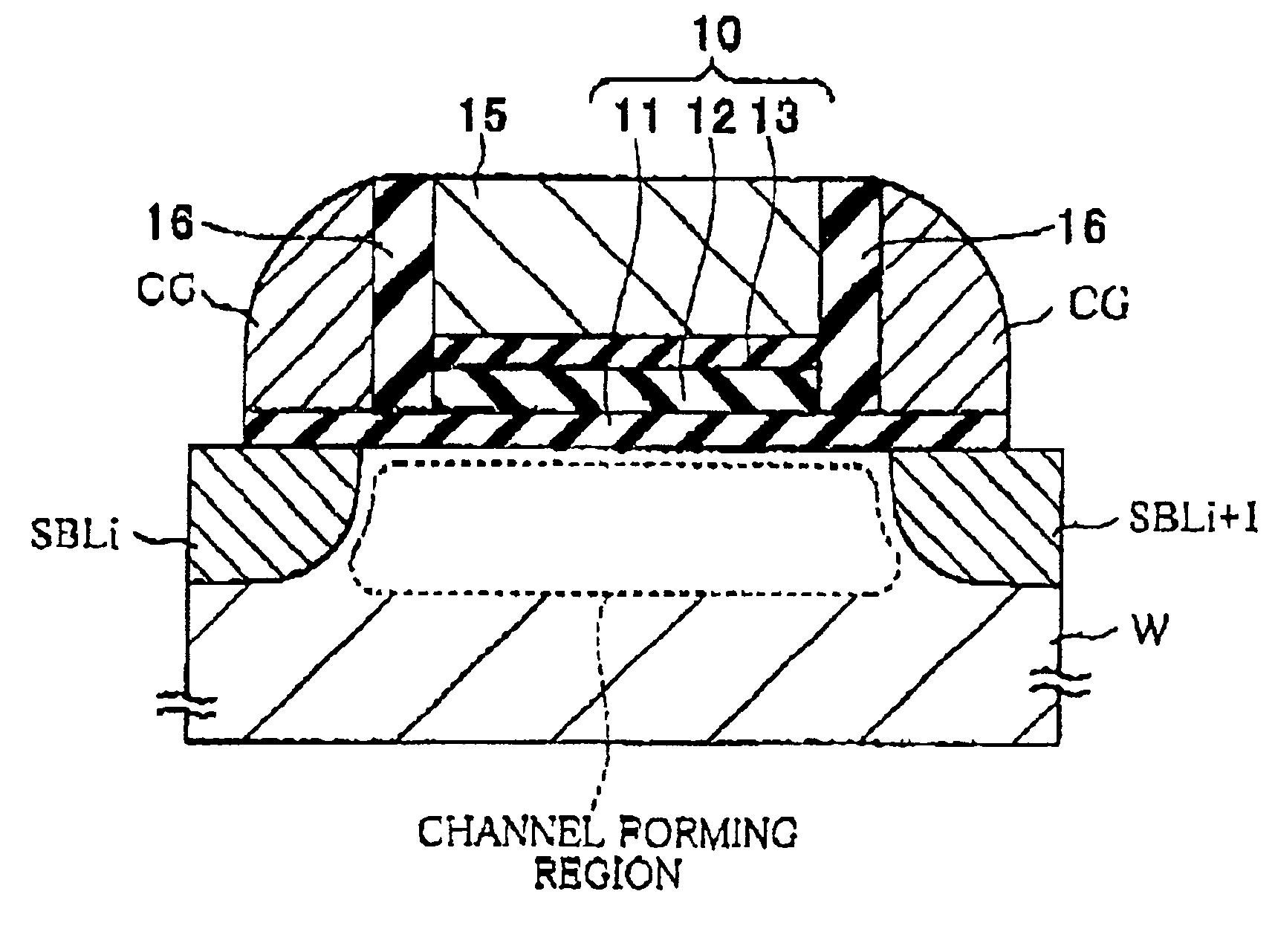
[0132]FIG. 10 is a cross-sectional view for illustrating the configuration of a memory transistor related to the second embodiment.

[0133]In this memory transistor, the gate insulating film consists of a gate insulating film 10a at the side of the sub-bit line SBLi and a gate insulating film 10b at the side of the sub-bit line SBLi+1. The two gate insulating films 10a and 10b are spatially separated by a single layer gate insulating film 14 above the central portion of the channel.

[0134]The gate insulating films 10a and 10b have the same structure as gate insulating film 10 in the first embodiment. That is, the gate insulating film 10a consists of a bottom insulating film 11a (FN tunnel...

third embodiment

[0149]The third embodiment relates to an application of the technique of FN tunneling low barrier to a transistor of a configuration comprising a second gate electrode, so-called control gate, at the source and / or drain side.

[0150]FIG. 11 and FIG. 12 are circuit diagrams of examples of configurations of memory cell arrays according to the third embodiment.

[0151]These memory transistor arrays are basically virtual grounding NOR type memory cell arrays the same as that in the fifth embodiment. But, in the present memory cell arrays, however, in each memory transistor, the control gates are provided to extend from the source and drain impurity region side to partly overlap with the channel forming region.

[0152]Further, the arrays are provided with a control line CL1a commonly connecting the control gates at one side of the memory transistors M11, M12, . . . connected in the bit line direction, a control line CL1b commonly connecting the control gates at the other side, a control line C...


PUM


Abstract

A nonvolatile semiconductor memory device having MONOS type memory cells of increased efficiency by hot electron injection and improved scaling characteristics includes a channel forming region in the vicinity of a surface of a substrate, first and second impurity regions, acting as a source and a drain in operation, formed in the vicinity of the surface of the substrate sandwiching the channel forming region between them, a gate insulating film stacked on the channel forming region and having a plurality of films, and a charge storing means that is formed in the gate insulating film dispersed in the plane facing the channel forming region. A bottom insulating film includes a dielectric film that exhibits a FN type electroconductivity and makes the energy barrier between the bottom insulating film and the substrate lower than that between silicon dioxide and silicon.

Description

BACKGROUND OF THE INVENTION[0001]1. Field of the Invention[0002]The present invention relates to a nonvolatile semiconductor memory device which has a planarly dispersed charge storing means (for example, in a MONOS type or a MNOS type, charge traps in a nitride film, charge traps near the interface between a top insulating film and the nitride film, small particle conductors, etc.) in a gate insulating film between a channel forming region and a gate electrode in a memory transistor and is operated to electrically inject primarily channel hot electrons, ballistic hot electrons, secondarily generated hot electrons, substrate hot electrons, and hot electrons caused by band-to-band tunneling current into the charge storing means to store the same therein and to extract the same therefrom and a method for operating the device.[0003]2. Description of the Related Art[0004]Nonvolatile semiconductor memories offer promise as large capacity, small size data-storage media. Along with the rec...

Claims


Application Information

Patent Timeline
IPC IPC(8): G11C11/40H01L29/76H01L21/02H01L21/70H01L29/66H01L27/115H01L21/318H01L21/82H01L21/8247H01L31/06H01L29/788H01L31/062H01L27/105H01L29/792G11C16/02G11C16/04G11C16/10H01L21/28H01L21/336H01L27/11568
CPCG11C16/0475G11C16/0491H01L21/28282H01L29/66833H01L29/792H01L29/40117
Inventor FUJIWARA, ICHIROKOBAYASHI, TOSHIO
Owner SONY CORP
Why Eureka
Try Eureka