Clock signal recovery circuit used in receiver of universal serial bus and method of recovering clock signal

a clock signal and universal serial bus technology, applied in the field of clock signals, can solve the problems of large dll circuit, large power consumption, and time delay in recovering the clock signal synchronized with the r_data

Inactive Publication Date: 2005-10-11
SAMSUNG ELECTRONICS CO LTD
View PDF4 Cites 24 Cited by
  • Summary
  • Abstract
  • Description
  • Claims
  • Application Information

AI Technical Summary

Benefits of technology

[0037]Advantageously, the present invention provides a mechanism for recovering a clock synchronized with data received from the USB transmitter within a short time (4-clock period).

Problems solved by technology

One disadvantage associated with the conventional PLL circuit is the time delay for recovering the RCCK signal synchronized with the R_DATA.
One disadvantage associated with the DLL method is that the DLL circuit comprises a multistage digital delay line and, consequently, the DLL circuit is large and consumes much power.

Method used


Image

  • Clock signal recovery circuit used in receiver of universal serial bus and method of recovering clock signal
  • Clock signal recovery circuit used in receiver of universal serial bus and method of recovering clock signal
  • Clock signal recovery circuit used in receiver of universal serial bus and method of recovering clock signal

Examples


Embodiment Construction

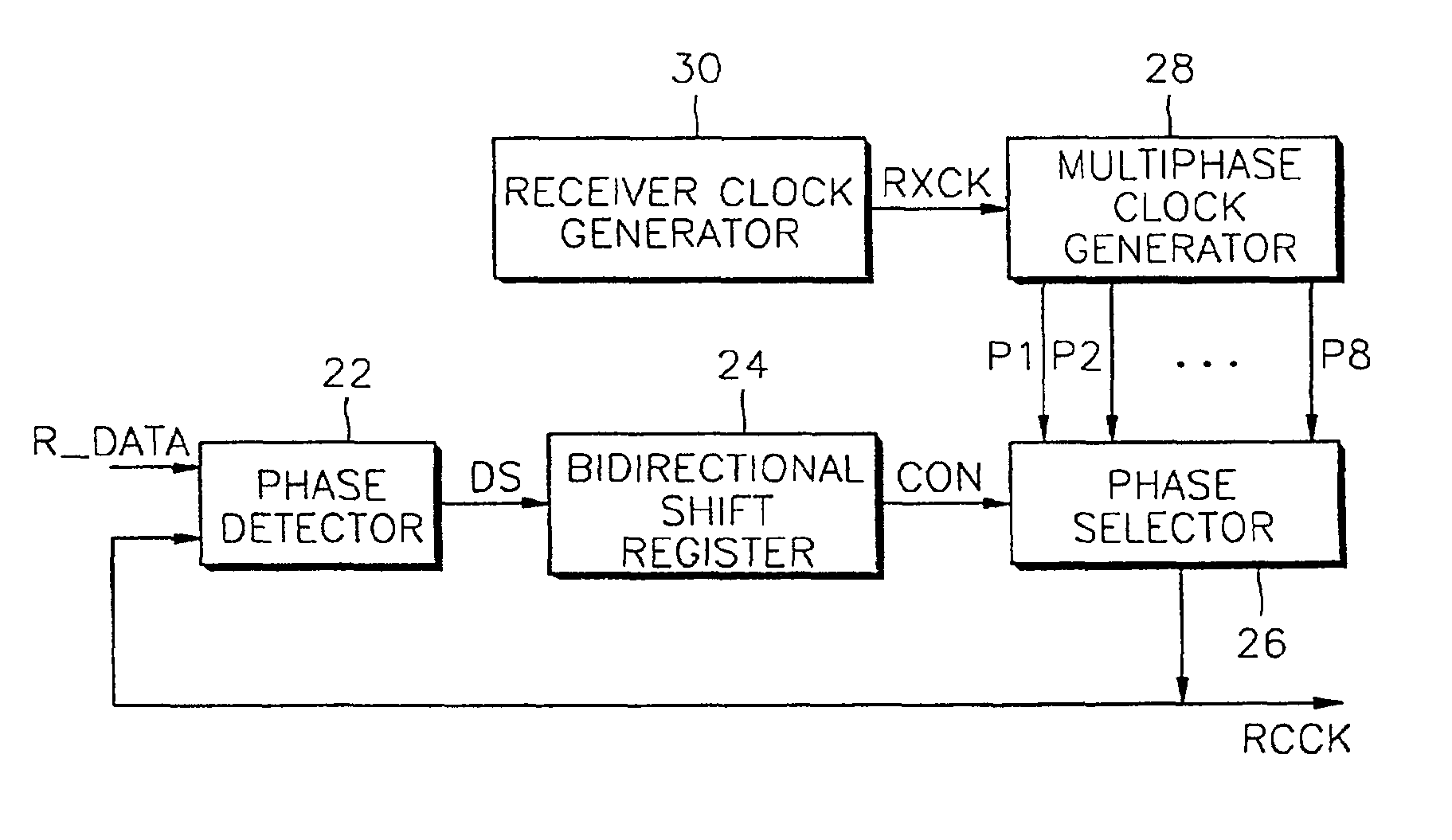
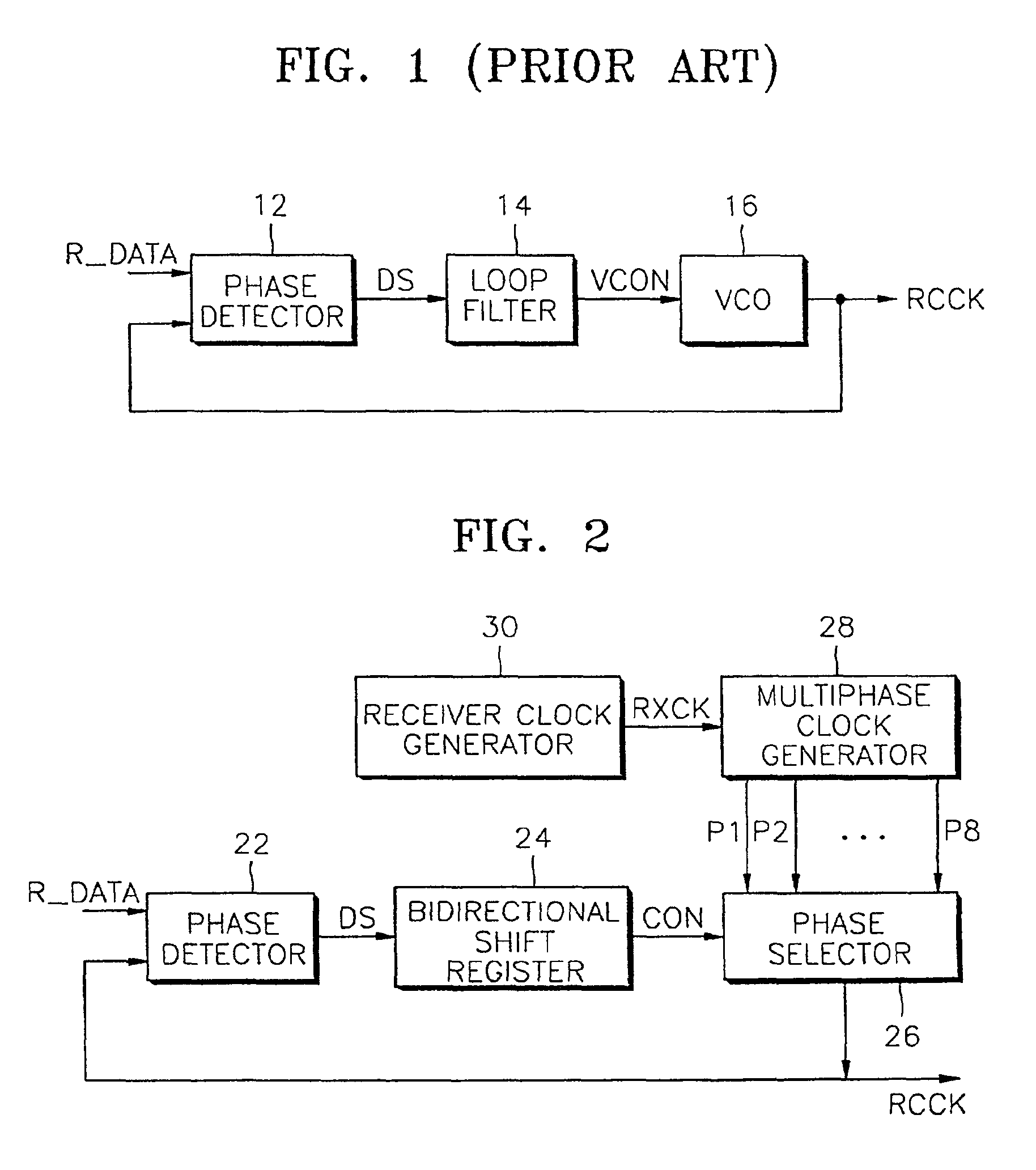
[0042]FIG. 2 illustrates a clock signal recovery circuit according to an embodiment of the present invention. A clock signal recovery circuit comprises a phase detector 22, a shift register 24, a phase selector 26, a multiphase clock signal generator 28, and a receiver clock signal generator 30. The phase detector 22 receives data R_DATA transmitted from a universal serial bus (USB) transmitter (not shown) via one terminal and a recovery clock (RCCK) signal via another terminal. The phase detector 22 compares and detects phases of two signals R_DATA and RCCK and generates a detected signal (DS). In response to the DS signal, the bidirectional shift register 24 is shifted in one of two directions to generate a control signal CON. In response to the control signal CON, the phase selector 26 selects one of a plurality of phase clock signals (e.g., P1 through P8) output from the multiphase clock signal generator 28 and outputs the selected phase clock signal as the RCCK signal.

[0043]The...


PUM


Abstract

A clock signal recovery circuit that is implemented in a receiver of a universal serial bus (USB) and a method for recovering a clock signal. The clock signal recovery circuit comprises a phase detector, a bidirectional shift register, a multiphase clock signal generator, and a phase selector. The phase detector detects a difference in phases between received data and a predetermined recovery clock signal and generates a first control signal indicative of the detected phase difference. The shift register is shifted in response to the detected signal and outputs a second control signal. The multiphase clock signal generator receives a receiver clock signal having the same frequency as that of a clock signal used in a USB transmitter (from which the data is transmitted) and generates a plurality of phase clock signals, preferably, first through N-th phase clock signals having the same frequencies as that of the receiver clock signal and having differences of about (360 / N)*I degree (°) (where N is an integer, and I is an integer equal to or greater than 0 and equal to or less than N−1) from a phase of the receiver clock signal, respectively. The phase selector selects one of the first through N-th phase clock signals in response to the second control signal and outputs the selected phase clock signal as the recovery clock signal. Preferably, N is an integer equal to or greater than 2 and equal to or less than 8.

Description

BACKGROUND OF THE INVENTION[0001]1. Technical Field[0002]The present invention relates generally to communications equipment, and more particularly, to a clock signal recovery circuit preferably implemented in a receiver of a universal serial bus (USB) and a method for recovering a clock signal.[0003]2. Description of Related Art[0004]A universal serial bus (hereinafter referred to as USB) is an interface standard for peripheral devices of a personal computer (PC). The implementation of USB affords integration of a plurality of interfaces for various peripheral equipment, thereby allowing a PC to be readily connected to a plurality of peripheral equipment at low cost. Consequently, USB has been employed for use with many types of PCs and peripheral equipment.[0005]A USB transmitter and a USB receiver (usually implemented in a single module, i.e., a USB transceiver) are necessary to communicate through the USB. In general, the same clock signal is used in the USB transmitter and the ...

Claims


Application Information

Patent Timeline
Patent Type & Authority Patents(United States)
IPC IPC(8): G06F13/42H04L7/033H03L7/00
CPCG06F13/4291H04L7/0337Y02B60/1228Y02B60/1235Y02D10/00H03L7/00
Inventor CHO, YOUNG-KYUN
Owner SAMSUNG ELECTRONICS CO LTD
Why Eureka
Try Eureka