Underfill for maximum flip chip package reliability

a flip chip and reliability technology, applied in the field of microelectronic technology, can solve the problems of increasing the power consumption of the chip, and increasing the complexity of the chip, so as to reduce cracking, and the effect of reducing the amount of chip shear

Inactive Publication Date: 2005-10-18
ALTERA CORP
View PDF4 Cites 27 Cited by
  • Summary
  • Abstract
  • Description
  • Claims
  • Application Information

AI Technical Summary

Benefits of technology

[0010]The present invention addresses the aforementioned problems by a novel method and apparatus for packaging electronic devices. In particular, the invention includes an underfill that has multiple regions of different stiffness. The underfill shell (the regions of the underfill that contact the top surface of the substrate and that contact the bottom surface of chip) is stiffer than the underfill bulk (the regions of the underfill that do not contact either the top surface of the substrate or the bottom surface of chip). The stiff underfill shell helps to minimize substrate warpage and chip shear and cracking due to the differing chip and substrate CTEs and the usually low tensile strengths of chips. The resilient underfill bulk is acceptable because the solder joints are usually composed of materials having high tensile strengths.

Problems solved by technology

One important characteristic of microelectronic technology is that over time integrated circuit geometry becomes smaller and smaller and circuitry density gets higher and higher, resulting in more powerful performance and more complex functionality per chip.
Even though the chip size keeps growing, the space left for each pad on the chip keeps shrinking.
The shrinkage of the chip pad area has reached a degree that exceeds the capability of traditional wire bond technology to make connections from the chip to the substrate.
However, the high cost of ceramic substrates limits their application to high-end products such as a CPU.
Because of the CTE difference between the chip and the substrate, the chip and the substrate bend to different degrees, causing thermal-mechanical stress and strain.
This thermal stress and strain concentrates on the solder joints between the chip and the substrate potentially causing early fatigue failure of the system if any solder joint is broken due to the thermal stress and strain concentration.
This problem is more prominent with organic substrates than with ceramic substrates.
Besides stress and strain concentration, another CTE-related issue is substrate warpage wherein the bottom surface of the substrate contracts more freely than the top surface of the substrate due to solder joint restraints from the chip, causing the substrate to bow into a convex shape.
However, for large flip chip substrates wherein the chip size could be several hundred square millimeters, the substrate warpage could easily exceed 8 mils, the standard set by the Joint Electron Device Engineering Council (JEDEC).
Excessive warpage of the substrate prevents the attachment of the substrate to the PCB and is one of many factors causing low yields.
Excessive warpage of the substrate may also cause chip shear and cracking because chip material generally has a low tensile strength.
This problem remains substantially unsolved after underfill curing because the existing underfill material, designed primarily to deal with stress and strain concentration on the solder joints, is relatively resilient and not stiff enough to provide the substrate the needed support to prevent warpage.

Method used


Image

  • Underfill for maximum flip chip package reliability
  • Underfill for maximum flip chip package reliability
  • Underfill for maximum flip chip package reliability

Examples


Embodiment Construction

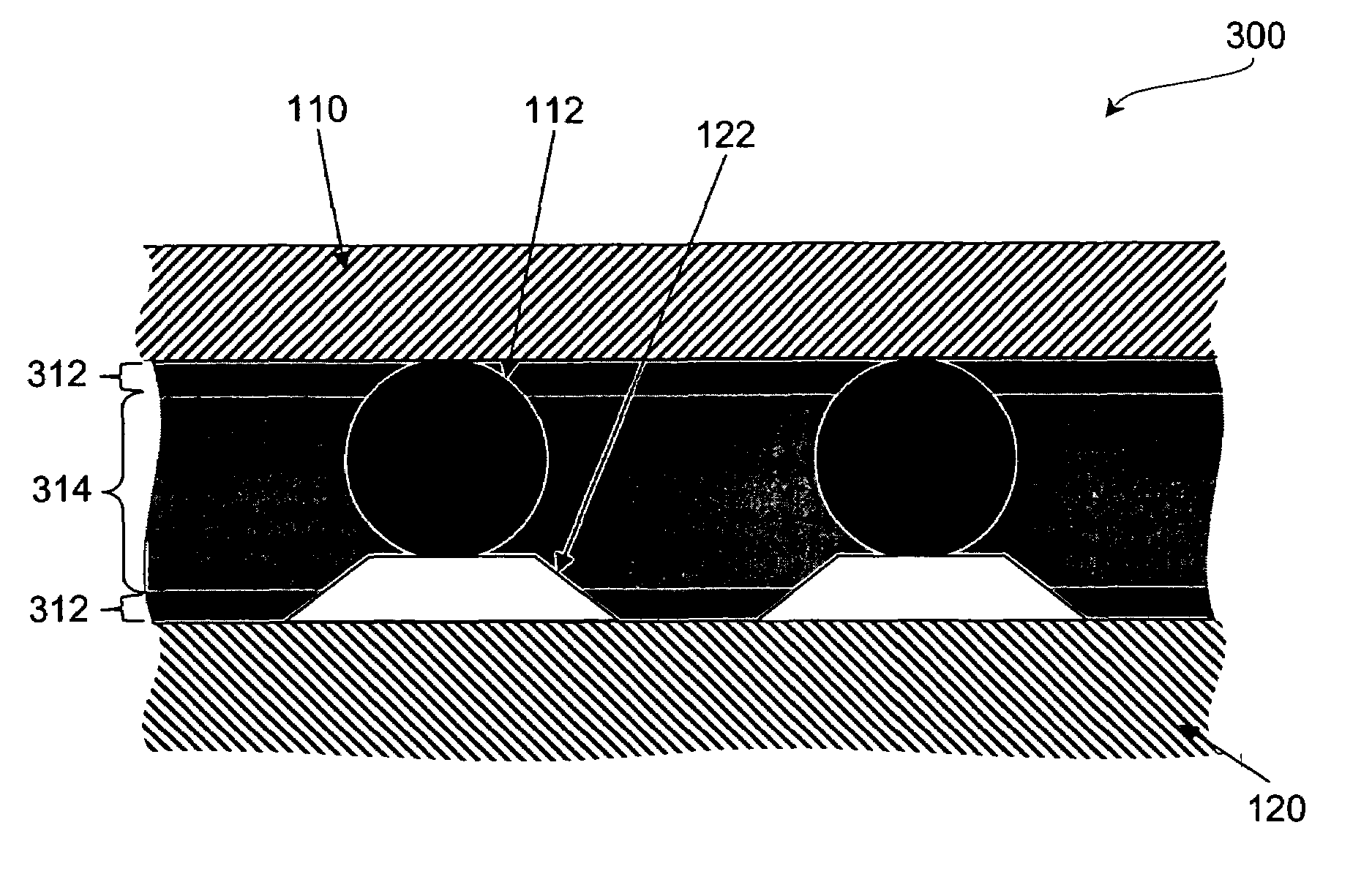
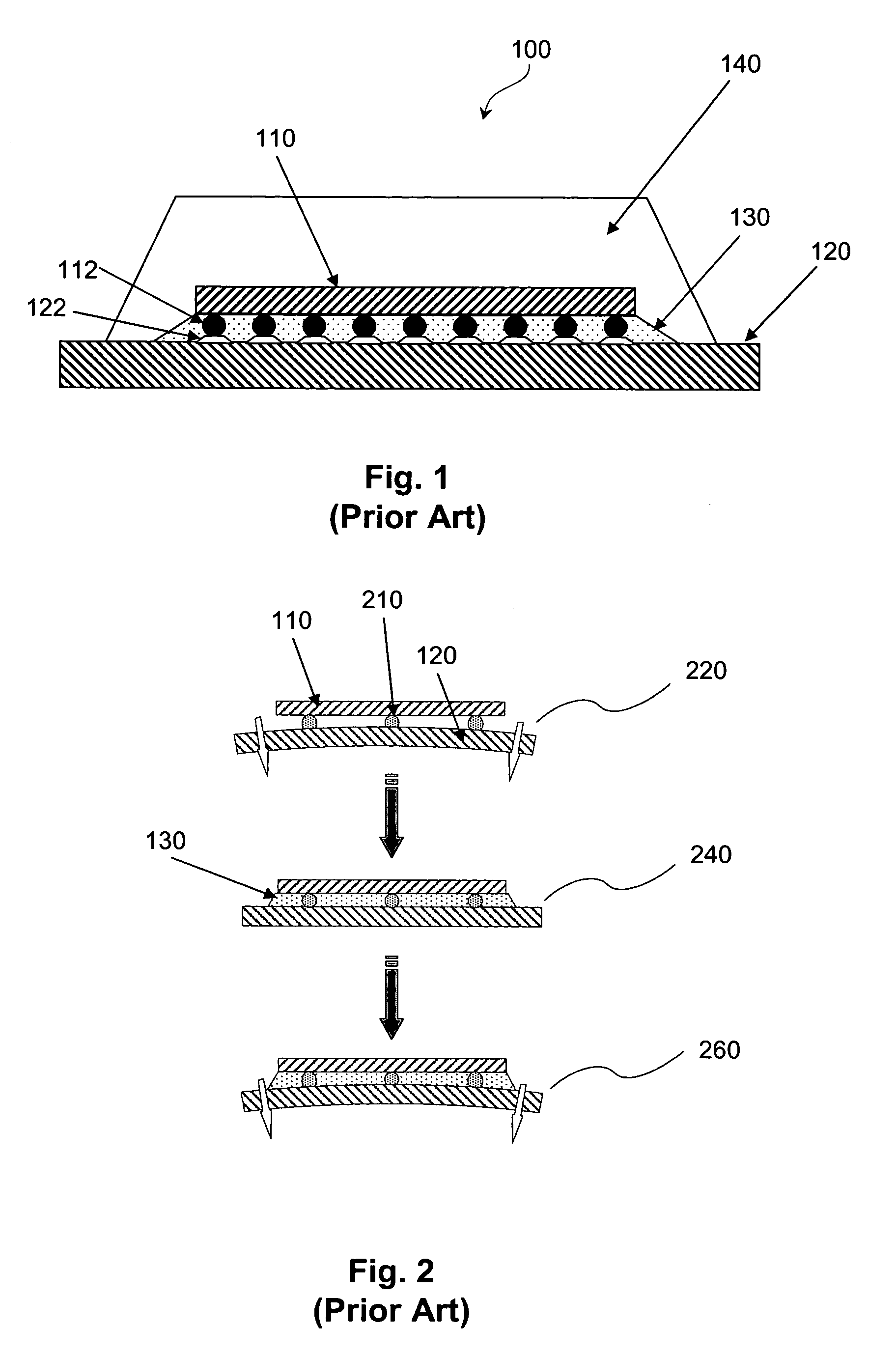
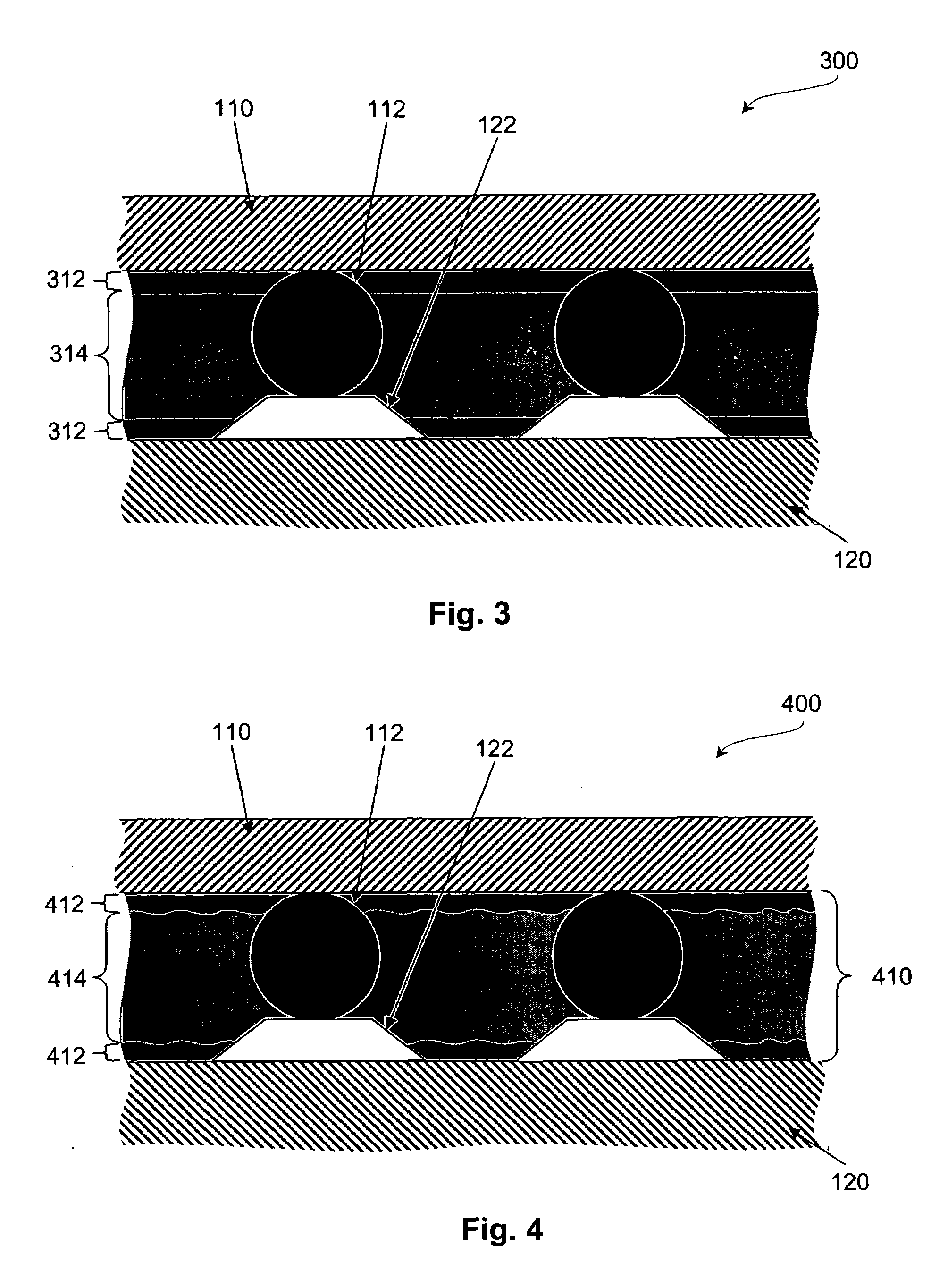
[0018]FIG. 1 shows a traditional FC package. A pattern of solder bumps or solder balls 112 is formed on one side of chip 110 that carries the integrated circuits (the bottom surface of chip 110). Chip 110 is flipped to the orientation shown in FIG. 1 and its pattern of solder bumps is aligned with the same pattern of solder pads 122 formed on substrate 120. Chip 110 is then lowered onto substrate 120 so that its solder bumps 112 contact solder pads 122 of substrate 120. Upon heating, the solder in bumps 112 and pads 122 flows together; and upon cooling, the solder forms solder joints that connect chip 110 to substrate 120. Then, underfill 130 and molding compound 140 are added to the package. As indicated above, the underfill typically is an epoxy-based polymer with a ceramic filler. The molding compound typically is silica-filled epoxy.

[0019]FIG. 2 is a schematic description of the thermomechanical deformation experienced by an organic substrate at different stages in an IC packagi...


PUM


Abstract

An electronic package is disclosed with an underfill with multiple areas of different stiffness and a method of constructing same. An underfill shell region that contacts the chip and the substrate is stiffer than an underfill build region that does not contact either the chip or the substrate. The variation in stiffness may be achieved using materials in the shell that include more filler and / or less solvents than the materials in the bulk region. The underfill may also be composed of a single material with an adhesion to the chip and substrate that is stronger than the material's internal cohesion (e.g., a long chain polymer with an active carboxyl group at the end of the chain). This can be achieved by exposing the chip and substrate surfaces to a curing substance (e.g., vaporized hydrofluoric acid).

Description

[0001]This invention relates generally to the packaging of semiconductor devices. More particularly, this invention relates to a semiconductor device package that minimizes the impact of different coefficients of thermal expansion (CTE) associated with the environment in which the package exists. The invention further relates to a unique underfill with multiple regions of different stiffness that reduces package warpage and chip shear and cracking due to internal thermal stress caused, for example, by differences in CTEs between different layers of the package.BACKGROUND OF THE INVENTION[0002]One important characteristic of microelectronic technology is that over time integrated circuit geometry becomes smaller and smaller and circuitry density gets higher and higher, resulting in more powerful performance and more complex functionality per chip. This dramatic performance and functionality improvement, in turn, requires many more input / output (I / O) connections between a chip and a p...

Claims


Application Information

Patent Timeline
Patent Type & Authority Patents(United States)
IPC IPC(8): H01L23/28H05K5/06H01L21/56
CPCH01L21/563H01L2224/73203H01L2924/3511H01L2224/16225H01L2224/32225H01L2224/73204H01L2924/00
Inventor HATA, WILLIAM Y.PASS, CHRISTOPHER J.
Owner ALTERA CORP
Why Eureka
Try Eureka