Apparatus for manufacturing stacked type electronic part

a technology of electronic parts and apparatus, which is applied in the direction of capacitor manufacturing, conductive pattern formation, coatings, etc., can solve the problems of inability to achieve practical productivity of manufacturing stacks of 100 to several hundred layers, difficult to embody as-is, and long time and positioning control in the movement of the jet head, etc., to achieve convenient practical use, increase manufacturing speed, and small

Inactive Publication Date: 2005-10-25
UHT CORP
View PDF13 Cites 27 Cited by
  • Summary
  • Abstract
  • Description
  • Claims
  • Application Information

AI Technical Summary

Benefits of technology

[0010]To increase productivity, each time an insulator layer and a conductor layer are formed, drying means drying the layers is needed. Temporary pressing means and holing means are required when necessary. In this case, in addition to the slurry jet head and the paste jet head, the drying means, temporary pressing means and holing means must be added. There are the disadvantages of lowered productivity, larger apparatus and higher equipment cost.
[0012]Another object of the present invention is to provide an apparatus for manufacturing a stacked type electronic part which is produced by increasing a manufacturing speed.
[0013]A further object of the present invention is to provide an apparatus for manufacturing a stacked type electronic part which is easily practically used and smaller by units of working means.
[0018]A plurality of insulator layer forming means and conductor layer forming means are juxtaposed. The base plate is moved back and forth in the linear section path in which they are arranged. A predetermined working is effectively performed in the steps of moving forth and moving back.
[0022]The arrangement of the insulator layer forming means, the conductor layer forming means and the drying means is suitably set according to the working steps such as the step of forming an insulator layer by an insulating resin paste and the step of forming a conductor layer by a conductor paste. The drying step by the drying means is frequent. At least one of one or more drying means is arranged in the substantially central part of the section, path, which is effective in the working efficiency.

Problems solved by technology

The disclosed technique of the publication has many practical problems as a specific apparatus and is difficult to embody as-is.
It takes a long time for time and positioning control in movement of the jet heads.
Practical productivity cannot be expected to manufacture a stack of 100 to several hundred layers.
The equipment cost is significantly high.
There are the disadvantages of lowered productivity, larger apparatus and higher equipment cost.

Method used


Image

  • Apparatus for manufacturing stacked type electronic part
  • Apparatus for manufacturing stacked type electronic part
  • Apparatus for manufacturing stacked type electronic part

Examples


first embodiment

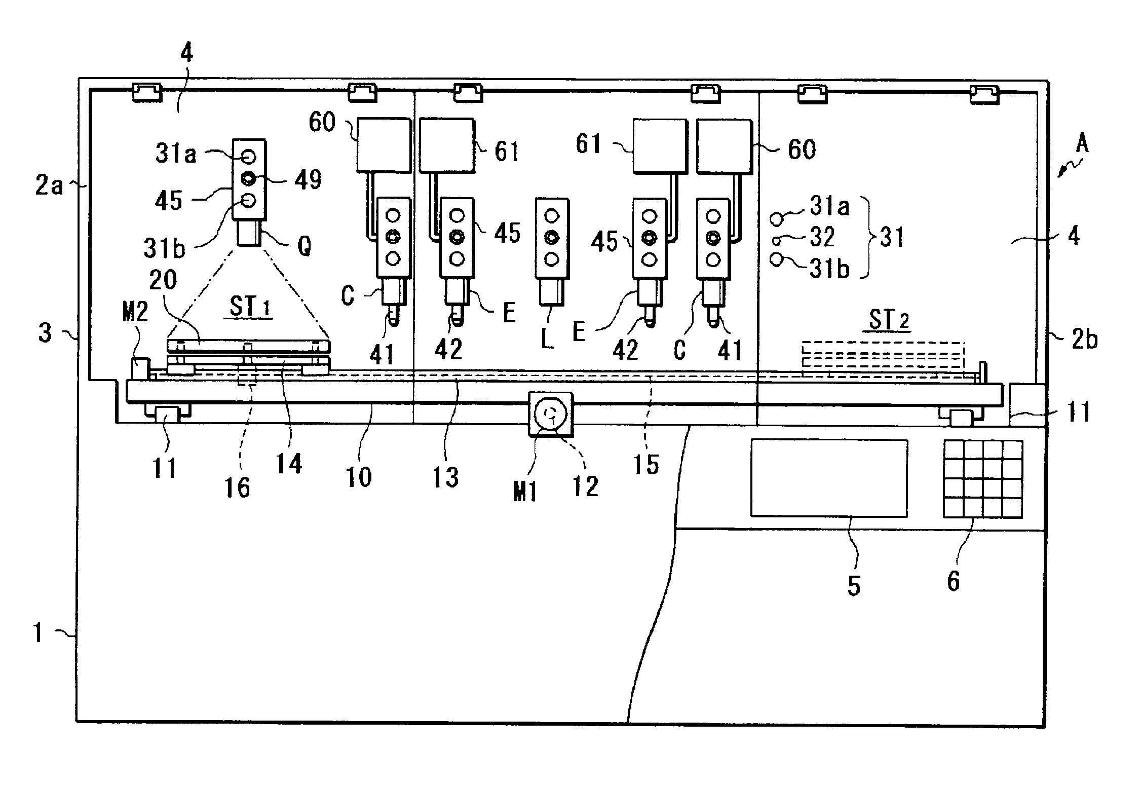
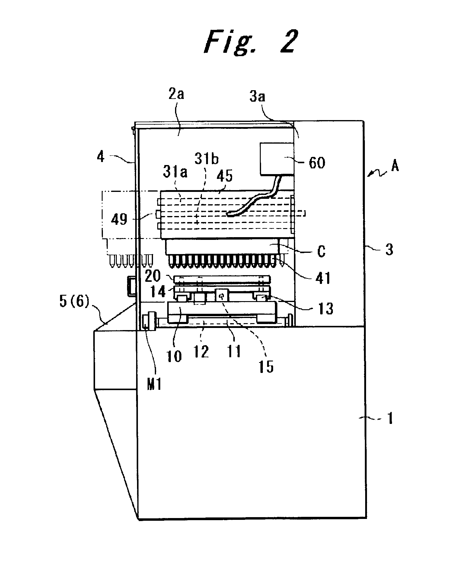
[0090]FIG. 1 shows the present invention in which the light irradiation unit L is disposed in the substantially central part of the section between the stages ST1 and ST2, the conductor paste jet unit E and the insulating resin paste jet unit C are arranged at its both sides, respectively, and the CCD camera unit Q is arranged above the stage ST1.

[0091]The numeral 60 shown in FIG. 1 denotes a paste layer supplying an insulating resin paste to the insulating resin paste jet unit C. The numeral 61 denotes a paste layer supplying a conductor paste to the conductor paste jet unit E.

[0092]In the first embodiment, an inductor and a stacked substrate as the stacked type electronic part are manufactured. Its working steps will be described in FIGS. 6A-6E.

[0093]In FIGS. 6A-6E, the base plate 20 is moved forth from the stage ST1 to the stage ST2 and moved back in the reverse direction. The light irradiation unit L, the conductor paste jet unit E, the insulating resin paste jet unit C and the ...

second embodiment

[0094]This point is the same in a second embodiment or after.

[0095]The following working steps are performed in the first embodiment.

[0096](A) When the base plate 20 is moved forth first, the left side insulating resin paste jet unit C and the light irradiation unit L are operated. The insulating resin paste jet unit C jets the insulating resin paste to form a base insulator layer 100 having a predetermined area on the base plate 20 (see FIG. 12). The light irradiation unit L dries the insulator layer 100 so as to bring it into a half-hardened state so as not to be tacky (see FIG. 17).

[0097](B) When the base plate 20 is moved back, the right side insulating resin paste jet unit C, conductor paste jet unit E, and the light irradiation unit L are operated.

[0098]The insulating resin paste jet unit C jets the insulating resin paste onto a region on the base insulator layer 100 except for a conductor pattern part (hereinafter, called an electrode pattern part) 102a to form a spacer insul...

third embodiment

[0119]FIGS. 8A-8D show the present invention in which an inductor is manufactured. The light irradiation units L are disposed in the substantially central part between the stages ST1 and ST2 and spaced at its right and left sides. The insulating resin paste jet unit C is arranged between the light irradiation units L, L at its one side (the stage ST1 side). The conductor paste jet unit E is arranged between the light irradiation units L, L at the other side. The camera unit Q is arranged above the stage ST1.

[0120]The following working steps are performed in the third embodiment.

[0121](A) When the base plate 20 is moved forth first, the insulating resin paste jet unit C, the conductor paste jet unit E and the central and right side light irradiation units L are operated.

[0122]The insulating resin paste jet unit C jets the insulating resin paste to form a base insulator layer 130 having a predetermined area on the base plate 20. The base insulator layer 130 is dried when passing below...


PUM

PropertyMeasurementUnit
widthaaaaaaaaaa
thicknessaaaaaaaaaa
thicknessaaaaaaaaaa

Abstract

An object of the present invention is to provide an apparatus for manufacturing a stacked type electronic part which can manufacture a stacked type electronic part dried at low temperature for a product by increasing a manufacturing speed. A base plate is placed in a predetermined linear section path to be moved back and forth and be moved vertically. Above the section path are juxtaposed one or more insulator layer forming means discharging an insulating resin paste, conductor layer forming means jetting a conductor paste by an ink jet system and drying means drying the pastes. A thin film layer having a predetermined conductor pattern placed on an insulator layer while the base plate is moved back and forth one or more times. Those steps are repeated to form a stacked type electronic part.

Description

BACKGROUND OF THE INVENTION[0001]1. Field of the Invention[0002]The present invention relates to an apparatus for manufacturing a stacked type electronic part. More specifically, the present invention relates to an apparatus for manufacturing a stacked type electronic part such as a stacked substrate (wiring substrate and package substrate), a capacitor, an inductor, a resistor and a magnetic material.[0003]2. Description of the Related Art[0004]A prior art stacked type electronic part has a required number of thin film layers deposited by repeating a forming step with a ceramics insulator layer and a predetermined electrode pattern. A method for stacking the thin film layers by omitting use of a resin carrier film which has been practically used as a base plate is proposed in Japanese Patent Application Laid-Open No. Hei 9-232174.[0005]In the publication, a base plate can be moved in X and Y directions by a mechanism using a servomotor and a ball screw. In place of that, a slurry j...

Claims


Application Information

Patent Timeline
Patent Type & Authority Patents(United States)
IPC IPC(8): H01L21/00H05K3/46H05K3/12H01F41/00H01G13/00
CPCH01L21/67092H01L21/6715H05K3/4664H01L21/67236H01L21/67173H05K3/1241H05K1/16
Inventor KAKIMOTO, MASAKAZUMATSUMOTO, FUMIAKIYASODA, HISASHIFURUTA, MAKOTO
Owner UHT CORP
Why Eureka
Try Eureka