Substrate for electro-optical device, electro-optical device and electronic apparatus

a technology of electrooptical devices and substrates, applied in the direction of luminescent screens, discharge tubes, identification means, etc., can solve the problem that the display screen seems to needlessly occupy a large surface area

Inactive Publication Date: 2005-10-25
BOE TECH GRP CO LTD
View PDF11 Cites 17 Cited by
  • Summary
  • Abstract
  • Description
  • Claims
  • Application Information

AI Technical Summary

Benefits of technology

[0010]In the substrate for the electro-optical device of the present invention, when controlled light is applied to the viewing side from the opposite side, light transmitted through the light-transmitting regions can achieve a proper display mode, and the controlled light can be cut off to permit observation of the mirror surface from the viewing side.
[0020]In the present invention, in the display mode, leaking light from regions other than the pixels can be prevented by the shielding layer to suppress decreases in contrast and chroma, and in the mirror mode, viewing of the mirror surface can be achieved by the shielding layer. Therefore, even in a relatively simple structure, both the display mode and the mirror mode can be achieved by effectively using the shielding layer.
[0022]In the present invention, light emitted from the pixels is substantially cut off to eliminate light which interferes with viewing of light reflected from the shielding layer, thereby achieving the visual effect of visualizing the mirror surface on the display screen. Therefore, the mirror mode can be achieved without a complicated structure.
[0026]In the present invention, the reflecting layer functions as the shielding layer for preventing decreases in contrast and chroma in the display mode using the controlled light transmitted through the light-transmitting regions, and functions as a component for forming the mirror surface when shielding light. Therefore, both functions (as the display member and as the mirror) can be achieved without complicating the structure.
[0030]In the present invention, as a whole, the mirror surface can be seen from the viewing side of the transparent substrate under a condition in which light transmitted through the light-transmitting regions is substantially cut off, and light which interferes with viewing of light reflected from the reflecting layer can thus be eliminated to achieve the visual effect of visualizing the mirror surface on the display screen. Therefore, the function as a mirror can be achieved without providing a complicated structure.

Problems solved by technology

The liquid crystal display panel having a relatively large display screen is not operated except at the time of mail communication and the start of telephone call, and thus the display screen seems to needlessly occupy a big surface area.

Method used


Image

  • Substrate for electro-optical device, electro-optical device and electronic apparatus
  • Substrate for electro-optical device, electro-optical device and electronic apparatus
  • Substrate for electro-optical device, electro-optical device and electronic apparatus

Examples


first embodiment

[0044

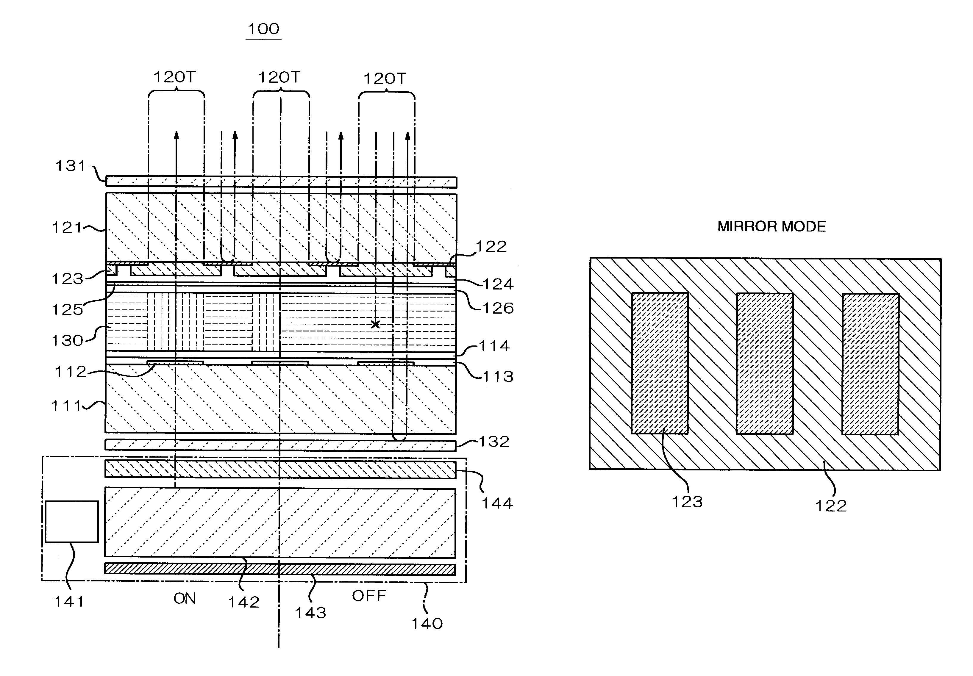
[0045]FIG. 1 is a schematic sectional view schematically showing the configuration of an electro-optical device (liquid crystal display) 100 according to a first embodiment of the present invention. The electro-optical device 100 of this embodiment has a panel structure in which substrates 111 and 121 each comprising a transparent material such as glass or plastic are bonded together with a sealing material (not shown in the drawing), and a liquid crystal 130 is sealed between the two substrates 111 and 121.

[0046]The substrate 111 includes electrodes 112 formed thereon comprising a transparent conductor such as ITO (Indium Tin Oxide) or the like. Furthermore, an insulating film 113 composed of SiO2 or TiO2 is formed on the electrodes 112, and an alignment film 114 comprising a polyimide resin is formed on the insulating film 113.

[0047]On the other hand, a reflecting layer 122 comprising a metal material or the like is formed on the substrate 121. The reflecting layer 122 is int...

second embodiment

[0061

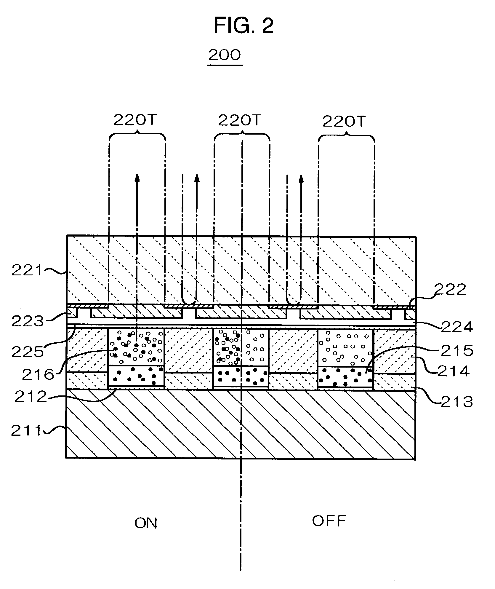
[0062]An electro-optical device according to a second embodiment of the present invention will be described with reference to FIG. 2. In this embodiment, a plurality of electrodes 212 each comprising ITO, a metal, a doped semiconductor layer, or the like are formed on a substrate 211 made of glass or silicon. Also, a partition comprising an insulating layer 213 composed of SiO2 or the like, and an insulating layer 214 composed of an organic resin or the like is provided in the spaces between the electrodes 212. Each of the electrodes 212 surrounded by the partition has a laminated structure comprising a hole injection / transport layer 215 and a luminescent layer 216.

[0063]As the material of the hole injection / transport layer 215, for example, a conductive polymer such as a polythiophene derivative, a polyaniline derivative, or the like, a low-molecular material such as a phenylamine derivative or the like can be used. As the material of the luminescent layer 216, an aromatic cyc...

third embodiment

[0070

[0071]An electronic apparatus comprising the electro-optical device 100 of the first embodiment according to a third embodiment of the present invention will be described in detail with reference to FIGS. 5 and 6. An electronic apparatus containing the electro-optical device 200 of the second embodiment can also be formed in the same manner as this embodiment.

[0072]FIG. 5 is a schematic block diagram showing the configuration of the display system of this embodiment. The electronic apparatus shown in FIG. 5 comprises the electro-optical device 100 of the first embodiment, a driving circuit 100D for driving the electro-optical device 100, and control means 300 for controlling the driving circuit 100D. In some cases (COG structure), the driving circuit 100D comprising, for example, a semiconductor IC or the like is mounted on the electro-optical device 100. The control means 300 comprises a display information output source 301, a display processing circuit 302, a power supply ci...


PUM

PropertyMeasurementUnit
distanceaaaaaaaaaa
distanceaaaaaaaaaa
transparentaaaaaaaaaa

Abstract

A substrate 121 has a reflecting layer 122 formed thereon, the reflecting layer 122 having a mirror surface on the substrate 121 side. When light is emitted from light transmitting regions 120T, a display mode is achieved in which a desired display mode is performed according to the state of the voltage applied to a liquid crystal 130. Also, when the voltage applied to the liquid crystal 130 is less than the threshold value, and a backlight 140 is turned off to substantially cut off light transmitted through all light-transmitting regions 120T, a mirror mode is set in which the entire surface is seen as a mirror surface by the mirror surface of the reflecting layer 122. Therefore, the display screen of the electro-optical device 100 can be used as a mirror.

Description

BACKGROUND OF THE INVENTION[0001]1. Technical Field of the Invention[0002]The present invention relates to a substrate for an electro-optical device, an electro-optical device, and an electronic apparatus.[0003]2. Description of the Related Art[0004]A liquid crystal display panel provided on a cellular phone or the like generally has a panel structure in which a liquid crystal is sealed between two substrates each comprising a transparent material such as glass, plastic, or the like. A backlight is disposed at the back of the panel structure, for illuminating the panel structure. The panel structure comprises a driving region in which pixels each comprising the liquid crystal and opposed electrodes (or electrode portions) disposed on both sides of the liquid crystal are arranged in a matrix to achieve a desired display mode. Furthermore, a shielding layer generally comprising a black resin or a metal is formed between the respective pixels in the driving region and in the peripheral...

Claims


Application Information

Patent Timeline
Patent Type & Authority Patents(United States)
IPC IPC(8): G02F1/1335G02F1/13H01J17/02H01J17/16G02B5/08G02B5/00G02B5/20G09F9/30G09F9/35H01L27/32
CPCG02F1/133553H01J17/16G02F2001/133562H01J2211/442H04M2201/38G02F1/133562G02F1/1335
Inventor TAKIZAWA, KEIJI
Owner BOE TECH GRP CO LTD
Why Eureka
Try Eureka