Quad state logic design methods, circuits, and systems

a logic design and circuit technology, applied in logic circuits, pulse techniques, instruments, etc., can solve the problems of power consumption of integrated circuits, wiring within integrated circuits as serious obstacle to the advancement of semiconductors, so as to reduce the wiring density of integrated circuits, reduce the effect of wiring interconnections and speed

Inactive Publication Date: 2005-11-08
TEXAS INSTR INC
View PDF4 Cites 12 Cited by
  • Summary
  • Abstract
  • Description
  • Claims
  • Application Information

AI Technical Summary

Benefits of technology

[0003]The present invention provides novel quad-state logic elements for use with quad-state memory elements to reduce the wiring density of integrated circuits. The present invention, among other features described herein, advantageously provides reduced wiring interconnects between memories and logic elements, resulting in higher speed, higher density, and lower power integrated circuit designs.

Problems solved by technology

As the density of integrated circuits tracks Moore's Law, the wiring within integrated circuit emerges as a serious obstacle to the advancement of semiconductors.
Also, as the number of signaling wires increase, power consumption of integrated circuits, related to charging and discharging of wiring capacitance, also increases and emerges as another serious obstacle to the advancement of semiconductors.

Method used


Image

  • Quad state logic design methods, circuits, and systems
  • Quad state logic design methods, circuits, and systems
  • Quad state logic design methods, circuits, and systems

Examples


Embodiment Construction

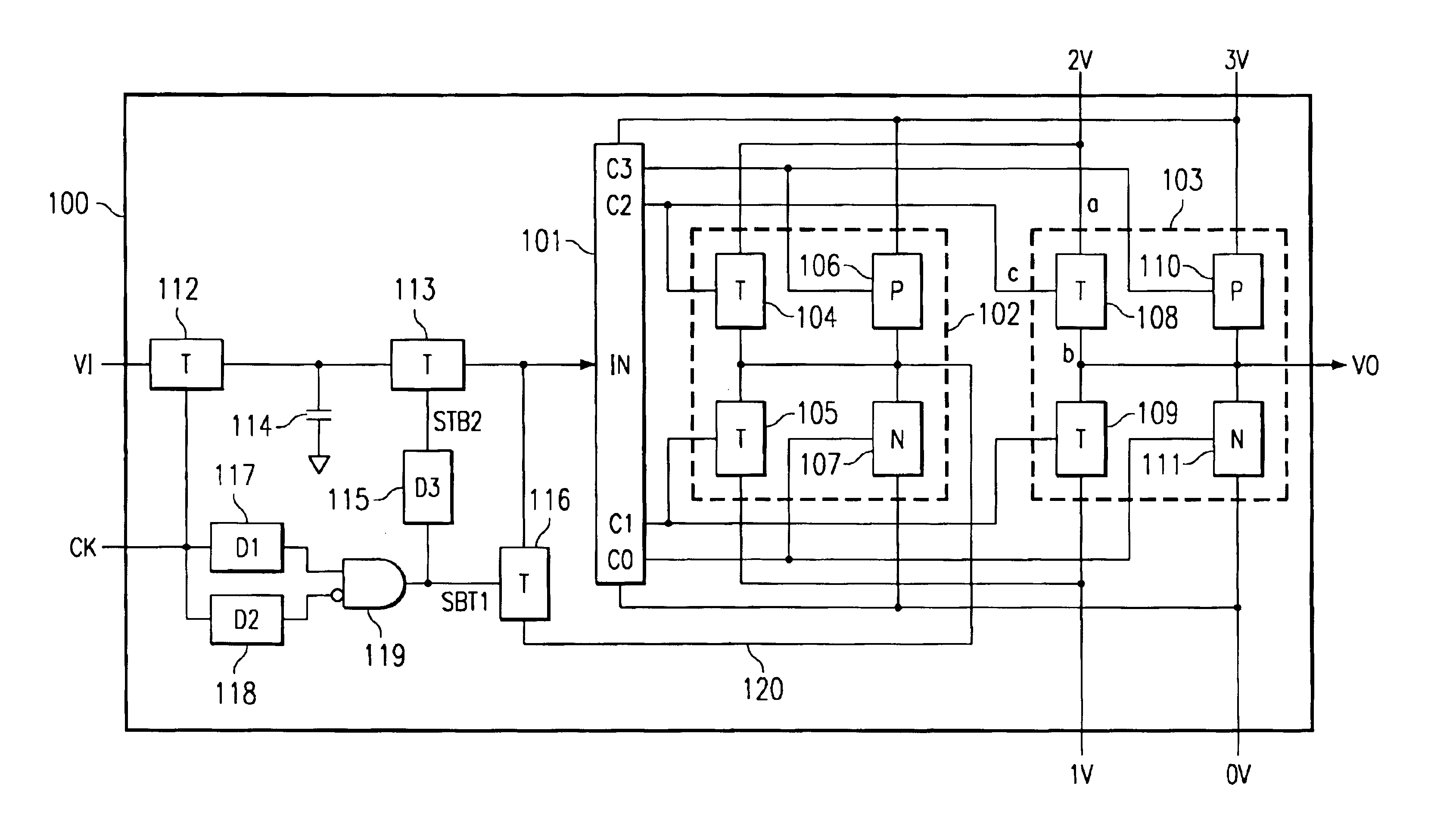
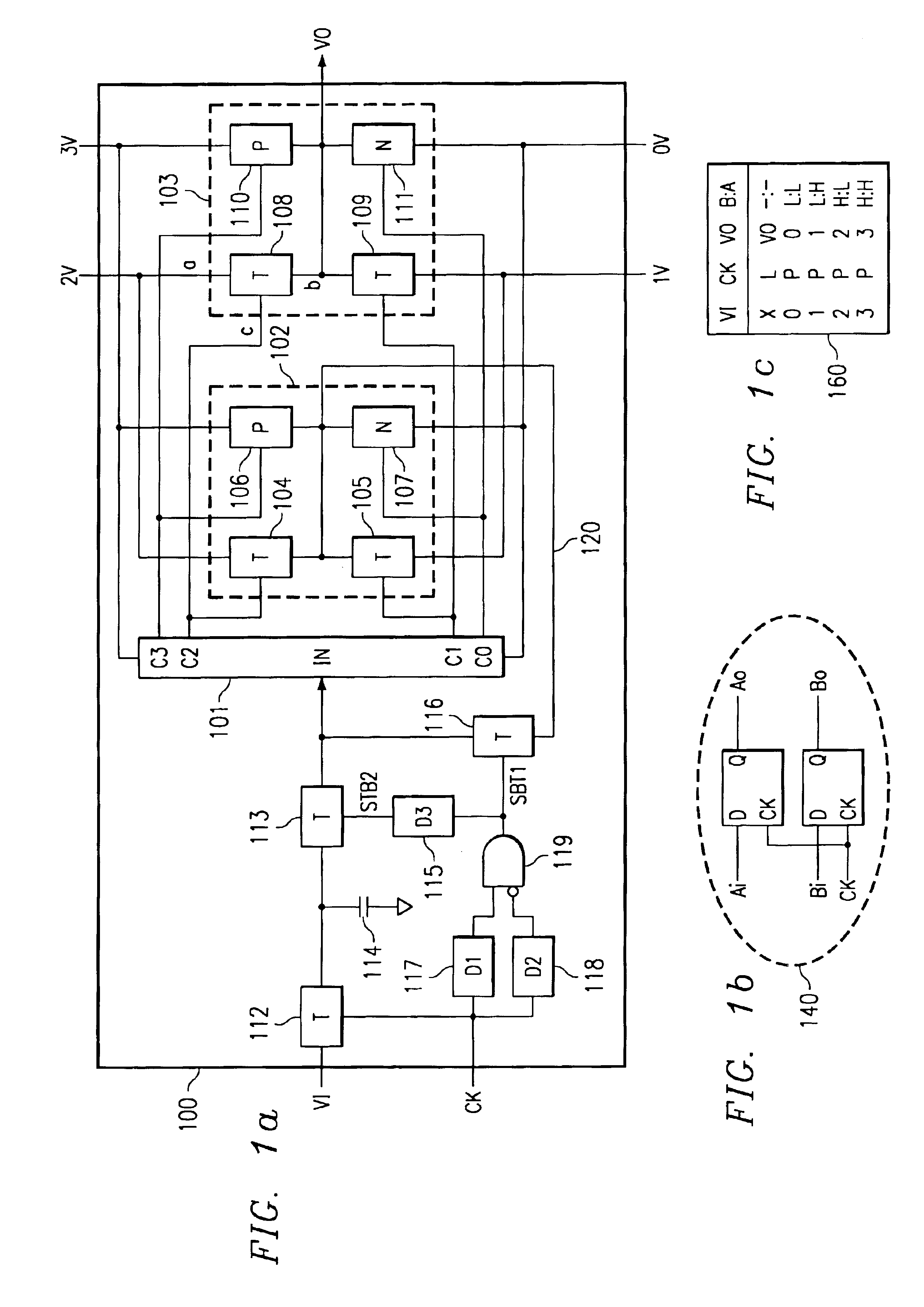
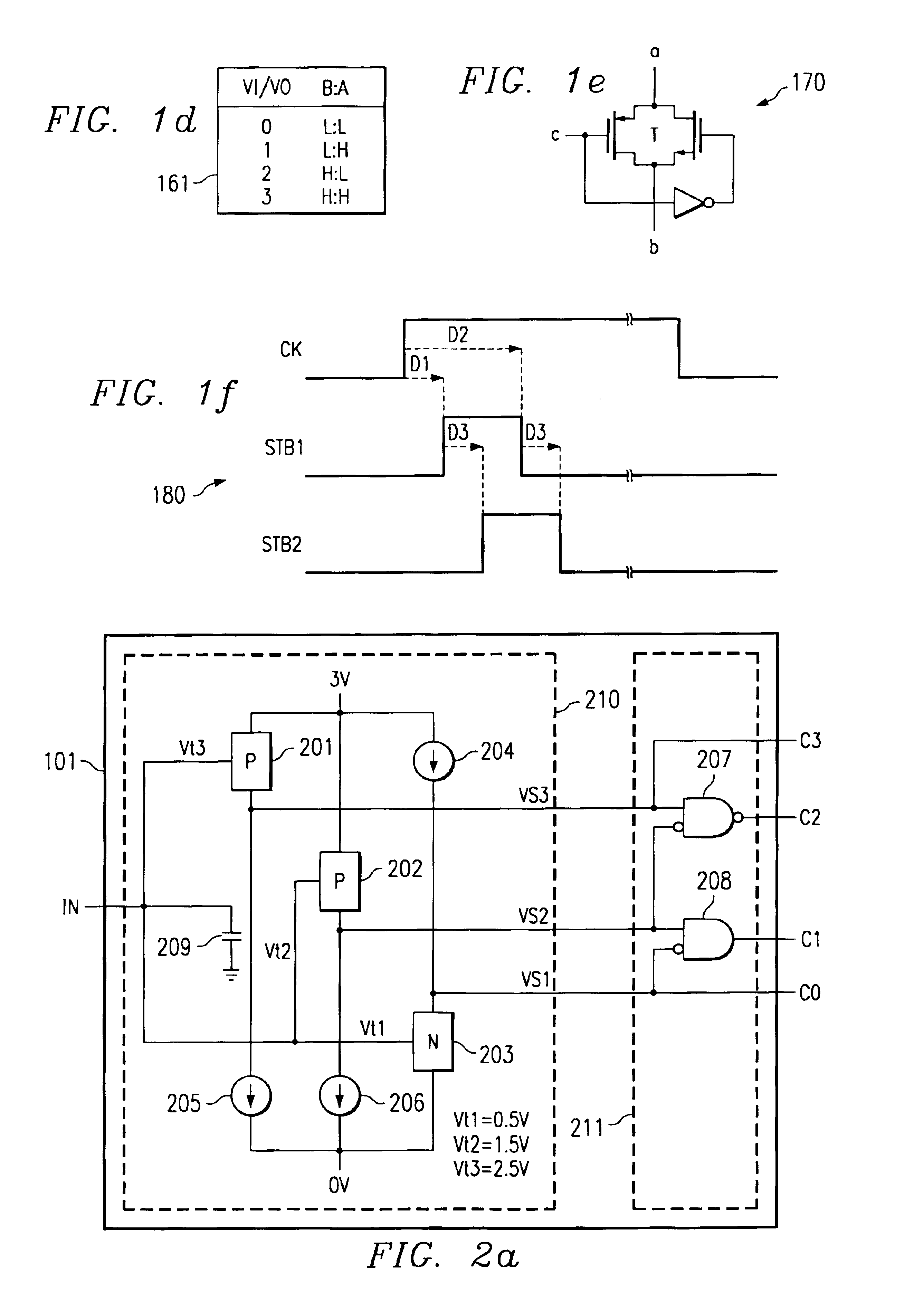
[0095]FIG. 1 illustrates an example circuit implementation of the quad state memory (QSM) 100 of the present invention. QSM 100 includes a voltage input (VI), a voltage output (VO), and a clock (CK) input. QSM 100 is connected to voltage supplies of 0V, IV, 2V, and 3V. Internally QSM 100 consists of a voltage to state converter 101, state feedback circuit 102, state output circuit 103, clock circuitry 117, 118, 119, 115, 116, VI transmission gates (T-gates) 112, 113, and 116, and VI holding capacitor 114. One lead of capacitor 114 is connected to the node between T-gates 112 and 113 and the other lead of capacitor 114 is connected to ground, which is equal to the 0V supply.

[0096]QSM 100 duplicates the memory functionality of the conventional D flip flop pair 140. While various types of D flip flops could be illustrated in 140, i.e. two phase level sensitive flip flops and single phase edge triggered flip flops, edge triggered types are shown. The VI input of QSM 100 is encoded by fo...


PUM


Abstract

Quad-state logic elements and quad-state memory elements are used to reduce the wiring density of integrated circuits. The resulting reduction in wiring interconnects between memories and logic elements results in higher speed, higher density, and lower power integrated circuit designs.

Description

[0001]This is a divisional application of Ser. No. 09 / 767,318 filed Jan. 22, 2001, which is now U.S. Pat. No. 6,636,076 which claims priority under 35 USC 119(e)(1) of provisional application Ser. No. 60 / 171,039, filed Dec. 16, 1999.BACKGROUND OF THE INVENTION[0002]Digital portions of integrated circuit designs consist generally of memories (i.e. flip flops / latches) for storing one of two logic states and connected gates (i.e. Boolean logic) for performing logical operations on the logic states stored in the memories. An N input logic gate may receive input from N memories via N separate wires. Moore's Law predicts that the number of transistors per square inch on integrated circuits doubles each 18 months. Thus, potentially the number of wires between memories and logic gates may double each 18 months. As the density of integrated circuits tracks Moore's Law, the wiring within integrated circuit emerges as a serious obstacle to the advancement of semiconductors. Also, as the number...

Claims


Application Information

Patent Timeline
Patent Type & Authority Patents(United States)
IPC IPC(8): H03K19/00
CPCG11C5/063G11C11/56H03K19/0002H03K19/1732
Inventor WHETSEL, LEE D.
Owner TEXAS INSTR INC
Why Eureka
Try Eureka