Active matrix type display apparatus method for driving the same, and display element

a display apparatus and active matrix technology, applied in the direction of identification means, instruments, static indicating devices, etc., can solve the problems of inability to obtain the effect of increasing the retention potential of a pixel electrode, the inability to reduce the voltage of a video signal driving circuit ic, and the inconsistency of the brightness gradient, etc., to achieve suppress horizontal crosstalk, reduce flickering or a brightness gradient, and high resolution

Inactive Publication Date: 2005-11-08
PANASONIC CORP
View PDF23 Cites 43 Cited by
  • Summary
  • Abstract
  • Description
  • Claims
  • Application Information

AI Technical Summary

Benefits of technology

[0172]According to the above-mentioned configuration, flickering or a brightness gradient can be reduced substantially in an active matrix type liquid crystal display apparatus. Furthermore, the above-mentioned configuration enables a pixel configuration of a dot inversion...

Problems solved by technology

However, in a liquid crystal display apparatus that changes the potential of a common electrode by the driving method as described in FIG. 15 with the circuit configuration in FIG. 3, the following becomes apparent: as a screen size increases, flickering and a brightness gradient (brightness inconsistency) occur conspicuously.
Therefore, in the case of the driving system in which a video signal with positive and negative polarities is applied while a scanning ele...

Method used


Image

  • Active matrix type display apparatus method for driving the same, and display element
  • Active matrix type display apparatus method for driving the same, and display element
  • Active matrix type display apparatus method for driving the same, and display element

Examples


embodiment 1

(Embodiment 1)

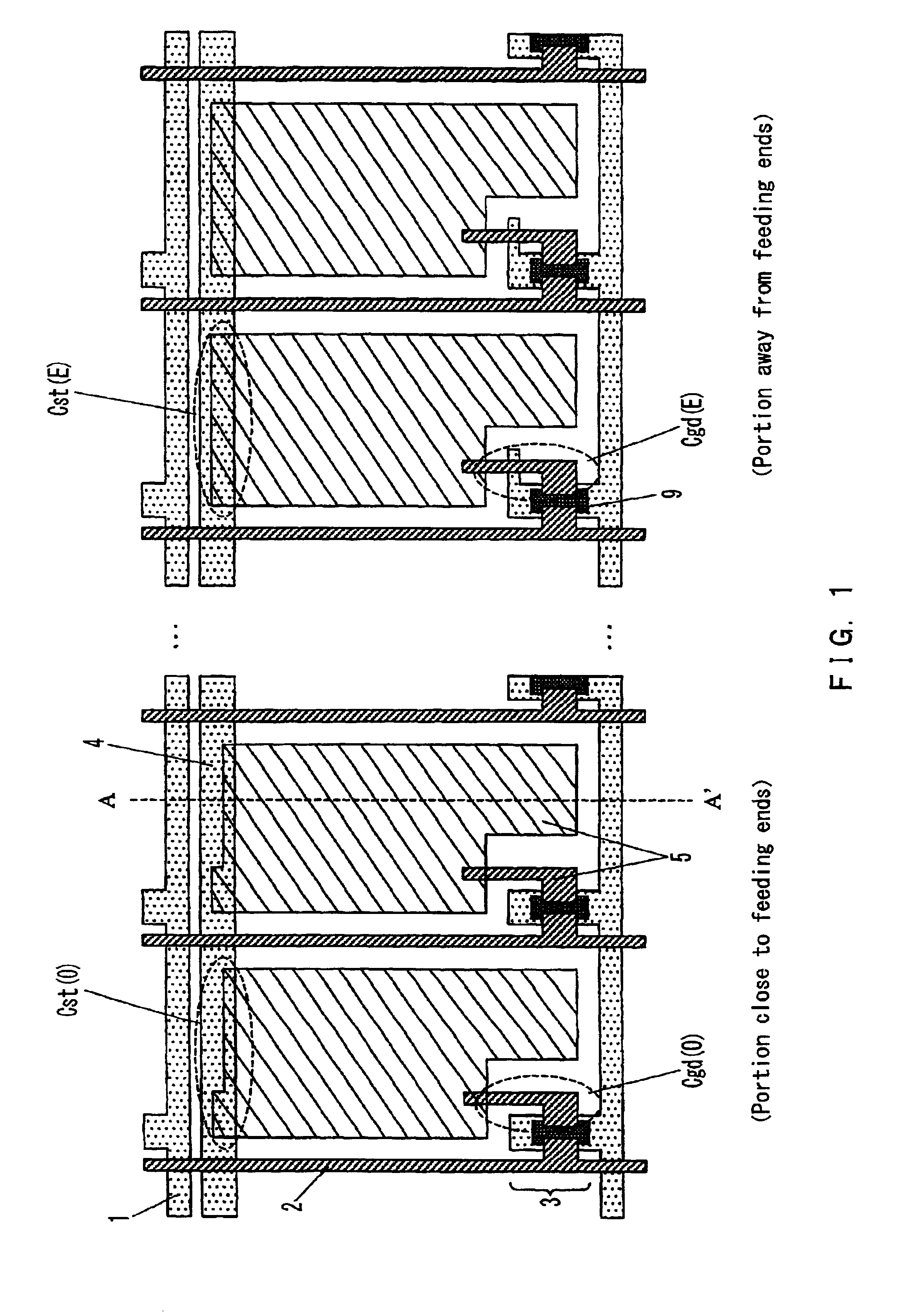
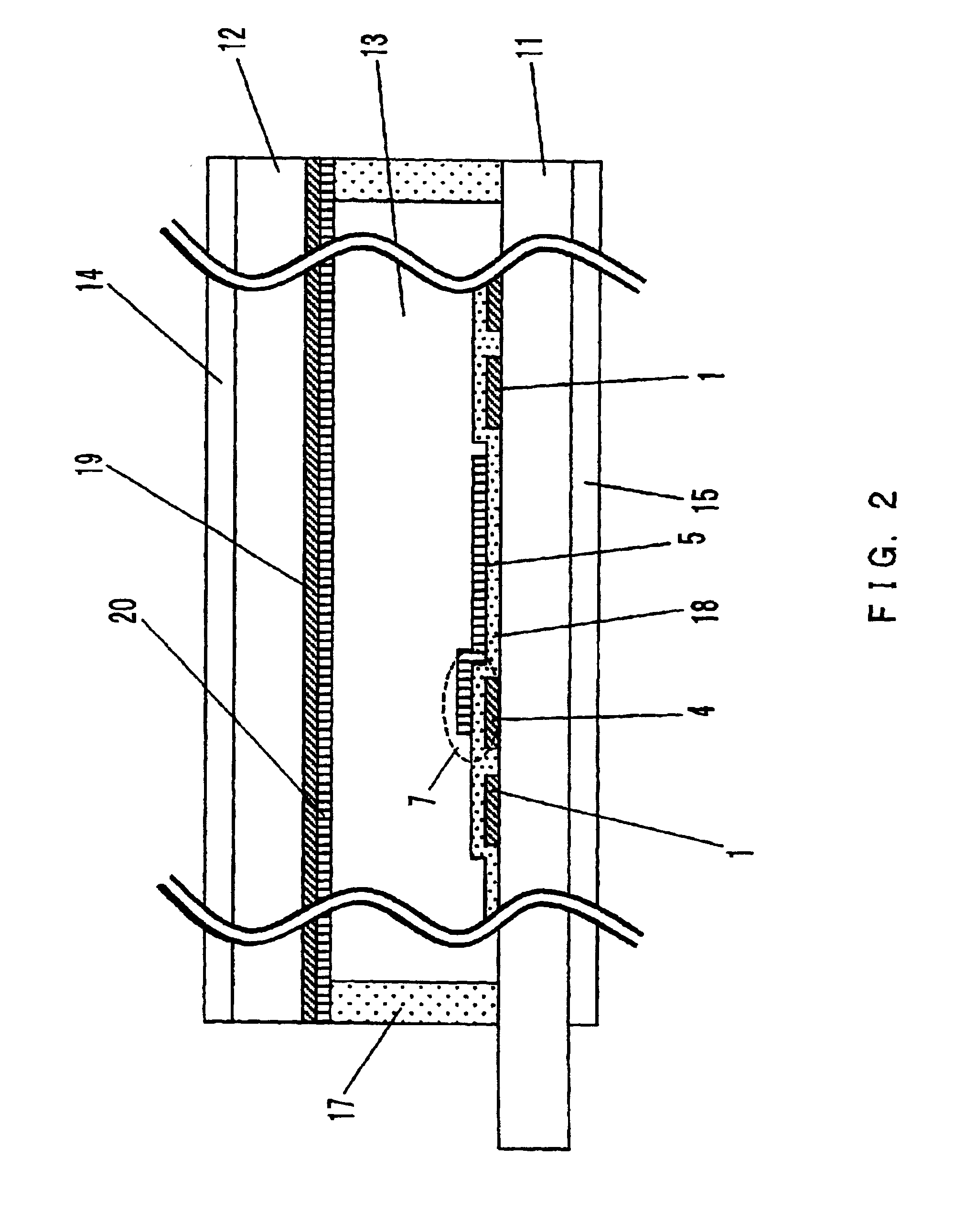
[0302]FIG. 1 is a plan view showing a pixel layout of a display apparatus of the first embodiment according to the present invention. FIG. 2 is a cross-sectional view taken along a line A-A′ in FIG. 1.

[0303]In FIGS. 1 and 2, reference numerals 11 and 12 denote substrates made of glass or the like. Reference numeral 11 denotes an array substrate on which thin film transistors 3 (also called TFTs or switching elements) and electrodes connected thereto are formed, and reference numeral 12 denotes a counter substrate opposing the array substrate. Liquid crystal 13 is interposed between two substrates as a display medium, and both ends of the substrates are sealed with a seal 17. Reference numerals 14 and 15 denote polarizing plates for conducting a polarization display, and 19 denotes a color filter for conducting a color display. Although the color filter 19 is formed on the counter substrate 12 side, it may be formed on the array substrate 11 side.

[0304]Scanning electrod...

embodiment 2

(Embodiment 2)

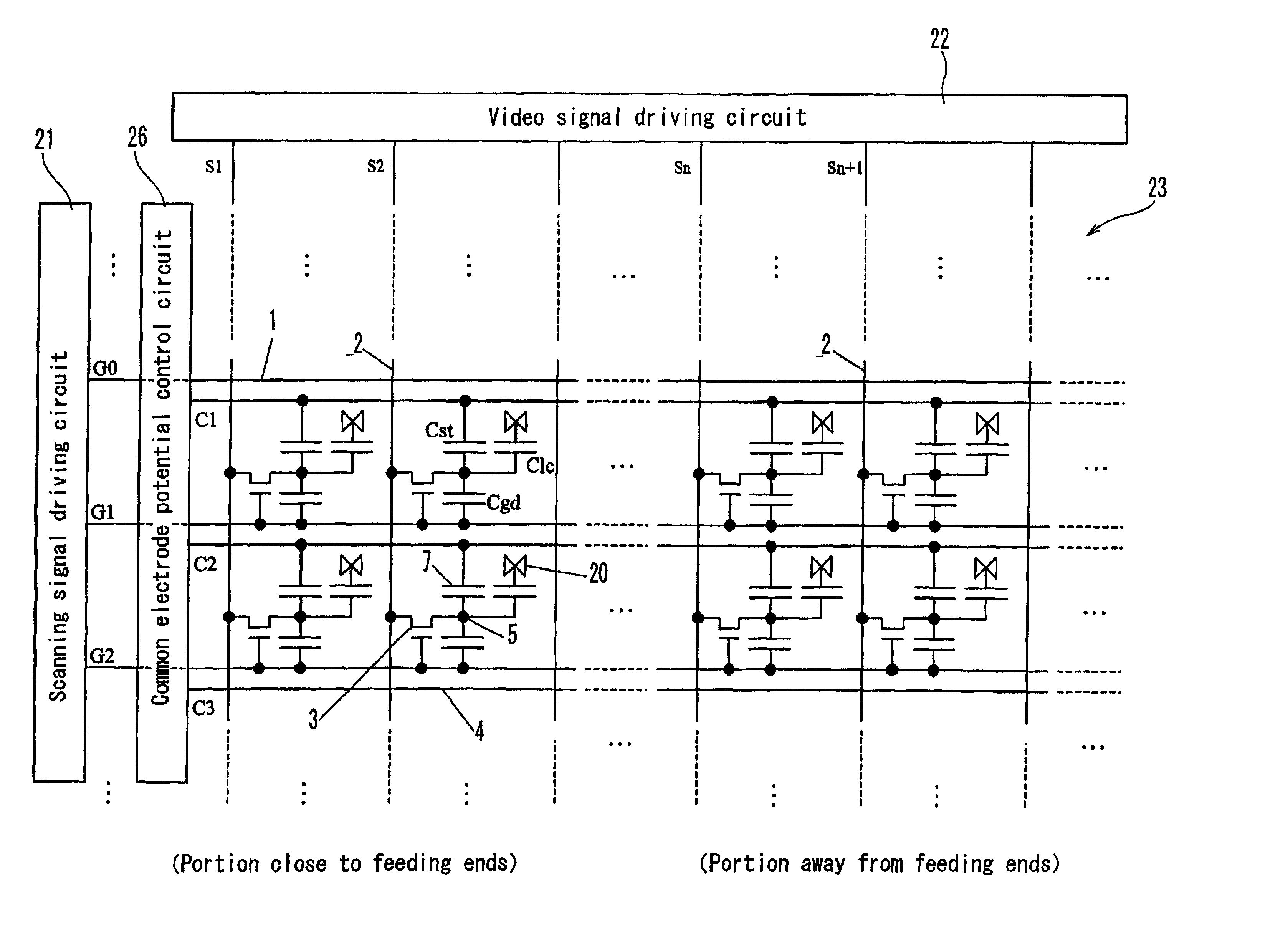
[0320]In Embodiment 2 of the present invention, the configuration that reduces horizontal crosstalk and lowers a voltage of a video signal driving circuit IC will be described with reference to FIGS. 4 and 5.

[0321]FIG. 4 is a plan view showing a pixel layout of a display apparatus of the second embodiment according to the present invention. The configuration in FIG. 4 basically follows the pixel layout in FIG. 1. In FIG. 4, pixels are inverted in the vertical direction per column. In this layout, in order not to disturb the symmetry in the vertical direction, a common electrode 4 is disposed in the middle between two scanning electrodes 1. An insulating film 18 (not shown) is interposed between the pixel electrode and the common electrode to form a storage capacitor 7 (Cst).

[0322]FIG. 5 is a circuit configuration diagram of a display apparatus of the second Embodiment according to the present invention. Basically, this also is the same as that in FIG. 3. However, pixel...

embodiment 3

(Embodiment 3)

[0329]According to the above-mentioned second embodiment, the effect of an increase in an amplitude of a pixel electrode retention potential as described in JP 5(1993)-143021 can be obtained with dot inversion driving or column inversion driving in the configurations of FIGS. 4 and 5. If this is allowed to proceed further, it is apparent that what is described in (Description 1 of the principle of the present invention: Principle of a reduction in a brightness gradient / flickering), (Principle 2 of the present invention: Optimum distribution of β and γ), (Supplementary item 1 regarding the principle: Vcp and ΔVcc), (Supplementary item 2 regarding the principle: method for supplying a power of scanning electrodes and common electrodes), and (Supplementary item 3 regarding the principle: Another circuit configuration) is adopted as it is, and predetermined effects such as a reduction in flickering, a decrease in a brightness gradient, and the like can be obtained.

[0330]Ac...


PUM


Abstract

An active matrix type display apparatus is provided that is inexpensive, has less crosstalk, has no flickering and a brightness gradient, and is suitable for a large screen size. The display apparatus includes a plurality of pixel electrodes arranged in a matrix, switching elements (TFTs) connected thereto, scanning electrodes, video signal electrodes, common electrodes, and a counter electrode, wherein liquid crystal, for example, is interposed between the pixel electrodes and the counter electrode. Assuming that a gate-drain capacitance is Cgd, a common electrode-pixel electrode capacitance is Cst, and the total capacitance connected to the pixel electrodes is Ctot in this configuration, αgd and αst represented by αgd=Cgd/Ctot, αst=Cst/Ctot are set to be different values between a portion close to feeding ends in a screen and a portion away therefrom.

Description

TECHNICAL FIELD[0001]The present invention relates to an active matrix type display apparatus using a switching element such as a thin film transistor, a method for driving the same, and a display element.BACKGROUND ART[0002]A display apparatus, for example, a liquid crystal display apparatus widely is used for various kinds of electronic equipment as a thin and light-weight flat display. In particular, an active matrix type liquid crystal display apparatus using a switching element such as a thin film transistor (TFT) actively is being applied to a monitor display for a personal computer, a liquid crystal TV, and the like due to its excellent image characteristics.[0003]First, the basic configuration of an active matrix type display apparatus will be described with reference to FIG. 3. The display apparatus roughly is composed of a scanning signal driving circuit 21, a video signal driving circuit 22, and a display element 23. The display element includes, as its main components, a...

Claims


Application Information

Patent Timeline
IPC IPC(8): G02F1/1343G02F1/1362G02F1/13G09G3/36G09G3/32G02F1/1368G02F1/133G02F1/1333G09F9/30G09F9/35G09G3/20G09G3/30H01L27/32H01L51/50H05B33/14H05B33/26H05B44/00
CPCG02F1/134336G02F1/136213G09G3/3648G09G3/3655G02F2001/133388G09G3/3233G09G3/3614G09G3/3659G09G2300/0842G09G2320/0209G09G2320/0219G09G2320/0223G09G2320/0247G02F1/133388G02F1/133
Inventor TANAKA, YUKIOKUMAGAWA, KATSUHIKOKIMURA, MASANORIKOMORI, KAZUNORI
Owner PANASONIC CORP
Why Eureka
Try Eureka